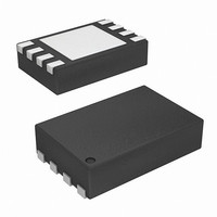
ISL9206ADRTZ-T Intersil, ISL9206ADRTZ-T Datasheet - Page 10

ISL9206ADRTZ-T
Manufacturer Part Number
ISL9206ADRTZ-T
Description
IC AUTHENTICATION DEVICE 8-TDFN
Manufacturer
Intersil
Series
FlexiHash+™r
Datasheet
1.ISL9206ADHZ-T.pdf
(17 pages)
Specifications of ISL9206ADRTZ-T
Function
Battery Authentication
Battery Type
Li-Ion, Li-Pol, NiMH
Voltage - Supply
2.6 V ~ 4.8 V
Operating Temperature
-25°C ~ 85°C
Mounting Type
Surface Mount
Package / Case
8-TDFN Exposed Pad
Lead Free Status / RoHS Status
Lead free / RoHS Compliant
Access Instruction Frame
The XSD access instruction frame is shown in Figure 9. The
instruction frame consists of 16 bits of digital signal with the
contents described in the following.
CS FIELD
The CS field is a 1-bit Chip Address Selection. An initial 1-bit
Chip Address code of ‘0’ is pre-programmed into the
device’s OTP ROM address location 0-00[7:6] at the time of
chip manufacture, and may be re-programmed by the pack
manufacturer if needed. If the CS code in the instruction
does not match the device’s Chip Address code, the
instruction, and any subsequent frames that follow, will be
ignored until a break command is received.
OPCODE FIELD
The OPCODE is a 2-bit field that defines the operation of the
transaction following the instruction frame. The operations
are described in Table 4.
BANK FIELD
The memories in the ISL9206A are divided into four banks.
The BANK field is defined in Table 5.
OPCODE
BANK
BYTES
FIELD
5 to 6
00
01
10
11
00
01
10
11
0
1
2
3
4
7
OTP ROM
Control and Status Registers
Device Authentication Registers
Test Registers (Reserved)
DATA BYTES
TO FOLLOW
Write Operation
Read Operation (normal)
Read Operation (with CRC) Read from device register. Append 1-Byte CRC to the end of the last read frame.
Sleep Mode Activation
TABLE 5. BANK FIELD DEFINITION.
MEMORY/REGISTER BANK SELECTION
N/A
N/A
16
DESCRIPTION
0
1
2
4
OTP ROM
WRITE
10
X
OTP ROM
Write to device register
Read from device register
Immediately sets the device in Sleep mode.
Note: After detecting the ‘11’ Opcode, the device immediately enters sleep mode. If more than 3 bits
sent, subsequent pulses may wake the device up again.
READ
X
X
X
TABLE 4. DEFINITION OF THE OPCODE FIELD
TABLE 6. DEFINITION OF THE BYTES FIELD
REG READ
OR WRITE
X
X
ISL9206A
CHLG CODE
WRITE
X
ADDRESS FIELD
The address field indicates the starting address of a memory
or register read or write sequence. Keep in mind that only odd
starting addresses are allowed for the OTP ROM access.
BYTES FIELD
The bytes field indicates the number of data bytes to read or
write, not including the CRC byte. Not all BYTES Field
settings are supported. Only settings marked with an ‘X’ are
valid for a particular bus instruction, as indicated in Table 6.
Attempting to read or write with an invalid BYTES setting
may yield unpredictable results.
Writing to OTP ROM can occur at only two bytes at a time,
but reading from OTP ROM can happen at 2, 4 or 16 bytes
at a time. Writing to and reading from OTP ROM in any other
byte denomination will yield unpredictable results and should
therefore be strictly prohibited.
Bus Transaction Protocol
The XSD bus for the ISL9206A defines three types of bus
transactions. Figure 10 shows the bus transaction protocol.
The blue color represents the signal sent by the host and the
green color stands for the signal sent by the device. Before
the transaction starts, the host should make sure that the
XSD device is not in the sleep mode. One method is to
always send a ‘break’ signal before starting the transaction,
as shown in Figure 10. If the device is not in the sleep mode,
the ‘break’ signal is not mandatory. The ‘break’ pulse width
may appear to be wider than what the host sends out
because of the reason explained in Figure 4. The symbols in
Figure 10 are explained in Table 7.
Invalid selection. Causes a bus error.
Must use 1-Byte read for clearing of the STAT register.
Invalid selection. Causes a bus error.
Invalid selection. Causes a bus error.
For reading from OTP ROM only (prior to lock-out).
ACTION
COMMENTS
July 30, 2008
FN6651.1


