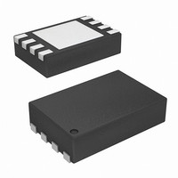
ISL9206ADRTZ-T Intersil, ISL9206ADRTZ-T Datasheet - Page 11

ISL9206ADRTZ-T
Manufacturer Part Number
ISL9206ADRTZ-T
Description
IC AUTHENTICATION DEVICE 8-TDFN
Manufacturer
Intersil
Series
FlexiHash+™r
Datasheet
1.ISL9206ADHZ-T.pdf
(17 pages)
Specifications of ISL9206ADRTZ-T
Function
Battery Authentication
Battery Type
Li-Ion, Li-Pol, NiMH
Voltage - Supply
2.6 V ~ 4.8 V
Operating Temperature
-25°C ~ 85°C
Mounting Type
Surface Mount
Package / Case
8-TDFN Exposed Pad
Lead Free Status / RoHS Status
Lead free / RoHS Compliant
Passive CRC Support
The CRC feature only supports the read transaction in the
ISL9206A. When the OPCODE in the instruction is ‘10’, an
8-Bit CRC is automatically calculated for the data bytes
being transferred out. The CRC result is then appended after
the last data byte is read out.
CRC is generated using the DOW CRC polynomial as
shown in Equation 1:
Polynom
SYMBOL
TABLE 7. SYMBOLS IN THE BUS TRANSACTION PROTOCOL
BREAK
BREAK
BREAK
IFG
IFG
TA
TA
break
break
break
H
D
H
D
STAGE
Stage
LSB
1st
1
LSB
ST
T
T
T
=
t
t
t
SD
SD
SD
SD
SD
Host inter-frame gap
Device inter-frame gap
Host turn-around time
Device turn-around time
SD
FIGURE 10. XSD BUS TRANSACTION PROTOCOL. THE ‘BREAK’ SIGNAL IS OPTIONAL IF THE DEVICE IS AWAKE
1
+
X
4
DESCRIPTION
STAGE
+
Stage
2
2nd
X
ND
5
+
X
8
READ INSTRUCTION FRAME
FIGURE 10C. BACK-TO-BACK TRANSACTION (READ FOLLOWED BY WRITE)
WRITE INSTRUCTION FRAME
READ INSTRUCTION FRAME
Read Instruction Frame
11
STAGE
Stage
3
3rd
FIGURE 11. THE CRC CALCULATOR FOR THE PASSIVE CRC SUPPORT
Write Instruction Frame
Read Instruction Frame
RD
0 BT
1 BT
MIN
STAGE
Stage
FIGURE 10A. MULTI-BYTE WRITE INSTRUCTION
4
FIGURE 10B. MULTI-BYTE READ INSTRUCTION
4th
TH
H
H
1 BT
1 BT
TYP
D
D
800ms
800ms
(EQ. 1)
MAX
ISL9206A
STAGE
Stage
5
5th
TH
The CRC generation algorithm is logically illustrated in
Figure 11. Prior to a new CRC calculation, the LFSR (linear
feedback shift register) is initialized to zero. The read data to
be transmitted out is concurrently shifted into the CRC
calculator. After the actual data is transmitted out, the final
content of the LFSR is the resulting CRC value. This value is
transmitted out after the read data, with LSB being
transmitted out first.
Analog Biasing Components and Clock Generation
The analog section of the ISL9206A mainly includes the
Time Base Generator and the internal regulator for powering
the circuits in the ISL9206A.
TIME BASE GENERATOR
A time base generator is included on-chip to provide timing
reference for serial data encoding and decoding at the XSD
bus interface. This eliminates the need for an external
crystal. The time base oscillator is trimmed during
manufacturing to a nominal frequency of 532.5kHz. It has a
frequency tolerance better than 5% over operating supply
voltage and temperature range.
TA
TA D
tA
tA
IFG H
tA
IFG
D
D
D
D
H
(OUPUT FROM SLAVE)
(OUPUT FROM SLAVE)
(output from slave)
(output from slave)
DATA FRAME 1
DATA FRAME 1
Data Frame
STAGE
Data Frame 1
Stage
6
DATA FRAME 1
6th
Data Frame 1
TH
STAGE
Stage
7
7th
TH
TA H
IFG D
tA
IFG
H
STAGE
Stage
IFG
H
MSB
IFG
MSB
8
D
8th
D
TH
(OUPUT FROM SLAVE)
NEXT INSTRUCTION
H
H
Next Instruction
(output from slave)
DATA FRAME 2
Data Frame 2
DATA FRAME 2
Data Frame 2
Frame
FRAME
SERIAL
DATA
Serial
Data
Output
July 30, 2008
Serial
FN6651.1


