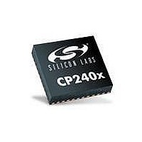
CP2401-GQ Silicon Laboratories Inc, CP2401-GQ Datasheet - Page 105

CP2401-GQ
Manufacturer Part Number
CP2401-GQ
Description
IC LCD DRIVER 48TQFP
Manufacturer
Silicon Laboratories Inc
Specifications of CP2401-GQ
Package / Case
48-TQFP, 48-VQFP
Display Type
LCD
Configuration
128 Segment
Interface
I²C, SMBus
Current - Supply
620µA
Voltage - Supply
1.8 V ~ 3.6 V
Operating Temperature
-40°C ~ 85°C
Mounting Type
Surface Mount
Data Ram Size
256 B
Interface Type
I2C, SMBus
Maximum Clock Frequency
25 MHz
Number Of Timers
2
Operating Supply Voltage
1.8 V to 3.6 V
Maximum Operating Temperature
+ 85 C
Mounting Style
SMD/SMT
Minimum Operating Temperature
- 40 C
Lead Free Status / RoHS Status
Lead free / RoHS Compliant
Digits Or Characters
-
Lead Free Status / Rohs Status
Lead free / RoHS Compliant
Other names
336-1860
Available stocks
Company
Part Number
Manufacturer
Quantity
Price
Company:
Part Number:
CP2401-GQ
Manufacturer:
Silicon Laboratories Inc
Quantity:
10 000
Part Number:
CP2401-GQ
Manufacturer:
SILICON LABS/芯科
Quantity:
20 000
Company:
Part Number:
CP2401-GQR
Manufacturer:
Silicon Laboratories Inc
Quantity:
10 000
CP2400/1/2/3
15.3. SMBus Operation
Two types of data transfers are possible: data transfers from a master transmitter to an addressed slave receiver
(WRITE), and data transfers from an addressed slave transmitter to a master receiver (READ). The master device
initiates both types of data transfers and provides the serial clock pulses on SCL. The SMBus interface on CP2401/
3 devices only supports slave receiver and slave transmitter modes.
A typical SMBus transaction consists of a START condition followed by an address byte (Bits7–1: 7-bit slave
address; Bit0: R/W direction bit), one or more bytes of data, and a STOP condition. Bytes that are received (by a
master or slave) are acknowledged (ACK) with a low SDA during a high SCL (see Figure 15.2). If the receiving
device does not ACK, the transmitting device will read a NACK (not acknowledge), which is a high SDA during a
high SCL.
The direction bit (R/W) occupies the least-significant bit position of the address byte. The direction bit is set to logic
1 to indicate a "READ" operation and cleared to logic 0 to indicate a "WRITE" operation.
All transactions are initiated by a master, with one or more addressed slave devices as the target.
The master
generates the START condition and then transmits the slave address and direction bit. If the transaction is a
WRITE operation from the master to the slave, the master transmits the data a byte at a time waiting for an ACK
from the slave at the end of each byte. For READ operations, the slave transmits the data waiting for an ACK from
the master at the end of each byte. At the end of the data transfer, the master generates a STOP condition to
terminate the transaction and free the bus. Figure 15.2 illustrates a typical SMBus transaction.
SCL
SDA
SLA6
SLA5-0
R/W
D7
D6-0
START
Slave Address + R/W
ACK
Data Byte
NACK
STOP
Figure 15.2. SMBus Transaction
15.3.1. Transmitter Vs. Receiver
On the SMBus communications interface, a device is the “transmitter” when it is sending an address or data byte to
another device on the bus. A device is a “receiver” when an address or data byte is being sent to it from another
device on the bus. The transmitter controls the SDA line during the address or data byte. After each byte of
address or data information is sent by the transmitter, the receiver sends an ACK or NACK bit during the ACK
phase of the transfer, during which time the receiver controls the SDA line.
15.3.2. Clock Low Extension
2
SMBus provides a clock synchronization mechanism, similar to I
C, which allows devices with different speed
capabilities to coexist on the bus. A clock-low extension is used during a transfer in order to allow slower slave
devices to communicate with faster masters. The slave may temporarily hold the SCL line LOW to extend the clock
low period, effectively decreasing the serial clock frequency.
Rev. 1.0
105


