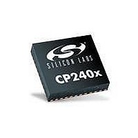
CP2401-GQ Silicon Laboratories Inc, CP2401-GQ Datasheet - Page 52

CP2401-GQ
Manufacturer Part Number
CP2401-GQ
Description
IC LCD DRIVER 48TQFP
Manufacturer
Silicon Laboratories Inc
Specifications of CP2401-GQ
Package / Case
48-TQFP, 48-VQFP
Display Type
LCD
Configuration
128 Segment
Interface
I²C, SMBus
Current - Supply
620µA
Voltage - Supply
1.8 V ~ 3.6 V
Operating Temperature
-40°C ~ 85°C
Mounting Type
Surface Mount
Data Ram Size
256 B
Interface Type
I2C, SMBus
Maximum Clock Frequency
25 MHz
Number Of Timers
2
Operating Supply Voltage
1.8 V to 3.6 V
Maximum Operating Temperature
+ 85 C
Mounting Style
SMD/SMT
Minimum Operating Temperature
- 40 C
Lead Free Status / RoHS Status
Lead free / RoHS Compliant
Digits Or Characters
-
Lead Free Status / Rohs Status
Lead free / RoHS Compliant
Other names
336-1860
Available stocks
Company
Part Number
Manufacturer
Quantity
Price
Company:
Part Number:
CP2401-GQ
Manufacturer:
Silicon Laboratories Inc
Quantity:
10 000
Part Number:
CP2401-GQ
Manufacturer:
SILICON LABS/芯科
Quantity:
20 000
Company:
Part Number:
CP2401-GQR
Manufacturer:
Silicon Laboratories Inc
Quantity:
10 000
CP2400/1/2/3
9.4.
In Ultra Low Power SmaRTClock Mode, the on-chip LDO is placed in a low power state and power is gated off from
all digital logic residing outside the ULP block. LCD functionality is disabled. The ULP block allows the device to
maintain a real time clock and detect SmaRTClock Alarm, SmaRTClock Oscillator Fail, and ULP Port Match
events. The Port Match functionality in ULP Mode differs from the functionality of Port Match when the device is in
normal or RAM Preservation Mode. See Section “9.7. Port Match Functionality in the Ultra Low Power Modes” on
page 56 for more details.
From normal mode, the device can be placed in ULP SmaRTClock Mode using the following procedure:
The device will not enter any ULP mode if there are pending wake-up events, and the INT pin will remain asserted.
To ensure that the device has successfully entered the low power mode, the host processor should verify that there
are no pending wake-up events prior to placing the device in a ULP mode and that the INT pin remains de-asserted
for 100 us after placing the device in ULP mode. If the INT pin is found to be asserted, then the host controller
should treat the situation as if the device has entered ULP and has been awoken by a wake-up event. The state of
RAM and unpreserved registers should not be relied upon since the host controller will not be able to determine if
the regulator has been disabled and re-enabled, or never disabled. The Port Match, SmaRTClock Alarm, and
SmaRTClock Oscillator Fail interrupts should always be enabled any time the device is placed in a ULP mode.
Once the device enters ULP SmaRTClock Mode, it will remain in this low power mode until a SmaRTClock Alarm,
SmaRTClock Oscillator Fail, or ULP Port Match wake-up event occurs. Once the device wakes up, it will generate
a reset complete interrupt and assert the INT pin. The host controller may also wake up the device at any time.
To resume normal mode operation, the host controller should use the following procedure:
Note: The Port I/O state and configuration settings are preserved as long as the device is in the low power mode. Upon wake-
In the ULP SmaRTClock Mode, the SmaRTClock oscillator may be disabled if a low frequency CMOS clock
(~32 kHz) is present at CLK pin. Set the RTCBYP bit (MSCN.7) to logic 1 in order to override the SmaRTClock with
the CMOS clock available at the CLK pin. The SmaRTClock should be disabled by writing 0x00 to the indirect
RTC0CN register instead of setting the RTCDIS bit (ULPCN.4). When the SmaRTClock is disabled, SmaRTClock
alarm and SmaRTClock oscillator fail detection functionality is no longer available.
52
up, all Port I/O state and configuration settings will reset, making all Port I/O digital inputs with weak pullups enabled.
They will remain in this state until the host controller re-initializes the Port I/O state and configuration registers.
Ultra Low Power SmaRTClock Mode
1. Set INT0EN:INT1EN to 0x1900. This enables the SmaRTClock Fail, SmaRTClock Alarm, and Port
2. Place the bandgap into its lowest power mode by writing 0x80 to MSCF.
3. Drive the PWR or NSS pin LOW.
4. Set the ULPEN (ULPCN.1) bit to logic 1. If port match functionality is not desired, ensure that all the
5. Drive the PWR or NSS pin HIGH.
1. Drive the PWR or NSS pin LOW.
2. Wait for the INT pin to be asserted. See Table 3.4 for ULP Mode wake up time.
3. Re-initialize all registers which are not preserved during ULP mode. See Table 6.3 for a list of registers
Match interrupts and disables all others.
ULP Port Mask bits are set to logic 0 by writing 1 to ULPRST (ULPCN.1).
that preserve their state in ULP mode.
Rev. 1.0


