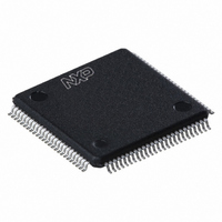
PCF2113DH/4,557 NXP Semiconductors, PCF2113DH/4,557 Datasheet - Page 18

PCF2113DH/4,557
Manufacturer Part Number
PCF2113DH/4,557
Description
IC LCD CONTROLLER/DRIVER 100LQFP
Manufacturer
NXP Semiconductors
Datasheet
1.PCF2113DH4557.pdf
(65 pages)
Specifications of PCF2113DH/4,557
Package / Case
100-LQFP
Display Type
LCD
Configuration
5 X 8 (Matrix)
Interface
I²C
Voltage - Supply
2.2 V ~ 4 V
Operating Temperature
-40°C ~ 85°C
Mounting Type
Surface Mount
Number Of Digits
40
Maximum Clock Frequency
450 KHz
Operating Supply Voltage
1.8 V to 5.5 V
Maximum Power Dissipation
400 mW
Maximum Operating Temperature
+ 75 C
Attached Touch Screen
No
Maximum Supply Current
50 mA
Minimum Operating Temperature
- 20 C
Operating Supply Voltage (typ)
2.5/3.3/5V
Package Type
LQFP
Pin Count
100
Mounting
Surface Mount
Power Dissipation
400mW
Operating Supply Voltage (min)
1.8V
Operating Supply Voltage (max)
5.5V
Lead Free Status / RoHS Status
Lead free / RoHS Compliant
Current - Supply
-
Digits Or Characters
-
Lead Free Status / Rohs Status
Lead free / RoHS Compliant
Other names
935276328557
PCF2113DH/4
PCF2113DH/4
PCF2113DH/4
PCF2113DH/4
Available stocks
Company
Part Number
Manufacturer
Quantity
Price
Company:
Part Number:
PCF2113DH/4,557
Manufacturer:
NXP Semiconductors
Quantity:
10 000
NXP Semiconductors
PCF2113_FAM_4
Product data sheet
Fig 11. Relationship between CGRAM addresses, data and display patterns
7
0
0
0
0
0
0
0
higher
order
6
bits
0
0
0
0
0
0
0
Character code bits 0 to 3 correspond to CGRAM address bits 3 to 6.
CGRAM address bits 0 to 2 designate the character pattern line position. The 8th line is the cursor position and display is
performed by logic OR with the cursor. Data in the 8th position appears in the cursor position.
Character pattern column positions correspond to CGRAM data bits 0 to 4, as shown in this figure.
CGRAM character patterns are selected when character code bits 4 to 7 are all logic 0. CGRAM data = logic 1 corresponds to
selection for display.
Only bits 0 to 5 of the CGRAM address are set by the ‘set CGRAM address’ command. Bit 6 can be set using the ‘set DDRAM
address’ command in the valid address range or by using the auto-increment feature during CGRAM write. All bits 0 to 6 can be
read using the ‘read busy flag’ and ‘address counter’ command.
character codes
(DDRAM data)
5
0
0
0
0
0
0
0
4
0
0
0
0
0
0
0
8.11 Character generator RAM
8.12 Cursor control circuit
3
0
0
0
1
1
1
1
2
0
0
0
1
1
1
1
lower
order
bits
Up to 16 user-defined characters may be stored in the Character Generator RAM
(CGRAM). Some CGRAM characters (see
icons (6 if icons blink and both icon rows are used in the application; 3 if no blink but both
icon rows are used in the application; 0 if no icons are driven by the icon rows). The
CGROM and CGRAM use a common address space, of which the first column is reserved
for the CGRAM (see
Figure 11
The cursor control circuit generates the cursor underline and/or cursor blink as shown in
Figure 12
When the address counter contains the CGRAM address the cursor will be inhibited.
1
0
0
1
1
1
1
1
0
0
1
0
1
1
1
1
1
1
1
1
0
6
0
0
shows the addressing principle for the CGRAM.
at the DDRAM address contained in the address counter.
higher
order
bits
1
1
1
1
0
0
0
5
0
0
1
1
1
1
1
4
CGRAM
address
3
0
1
0
1
1
1
1
Figure
0
0
0
0
1
1
1
1
0
0
0
0
1
1
1
1
0
0
1
1
1
1
2
lower
order
bits
Rev. 04 — 4 March 2008
0
0
1
1
0
0
1
1
0
0
1
1
0
0
1
1
0
0
0
0
1
1
1
0
0
1
0
1
0
1
0
1
0
1
0
1
0
1
0
1
0
1
0
1
0
1
7,
Figure
higher
order
bits
8,
Figure 9
4
0
0
0
0
0
0
character patterns
Figure 18
(CGRAM data)
3
0
0
0
0
0
0
0
0
0
0
0
2
0
0
0
0
0
0
0
0
lower
order
and
bits
1
0
0
0
0
0
0
0
0
0
0
and
Figure
0
0
0
0
0
0
0
0
0
0
0
Figure
example 1
example 2
character
character
pattern
position
pattern
cursor
10).
19) are also used to drive
LCD controllers/drivers
PCF2113x
4
1
1
1
1
1
1
1
0
1
0
1
0
1
0
0
0
© NXP B.V. 2008. All rights reserved.
character code
(CGRAM data)
3
1
0
0
1
0
0
0
0
0
1
1
0
1
0
0
0
2
1
0
0
1
1
0
0
0
0
0
1
1
1
1
1
0
1
1
0
0
1
0
1
0
0
0
1
1
0
1
0
0
0
mge995
0
0
1
1
0
0
0
1
0
1
0
1
0
1
0
0
0
18 of 65


