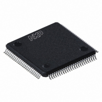
PCF2113DH/4,557 NXP Semiconductors, PCF2113DH/4,557 Datasheet - Page 28

PCF2113DH/4,557
Manufacturer Part Number
PCF2113DH/4,557
Description
IC LCD CONTROLLER/DRIVER 100LQFP
Manufacturer
NXP Semiconductors
Datasheet
1.PCF2113DH4557.pdf
(65 pages)
Specifications of PCF2113DH/4,557
Package / Case
100-LQFP
Display Type
LCD
Configuration
5 X 8 (Matrix)
Interface
I²C
Voltage - Supply
2.2 V ~ 4 V
Operating Temperature
-40°C ~ 85°C
Mounting Type
Surface Mount
Number Of Digits
40
Maximum Clock Frequency
450 KHz
Operating Supply Voltage
1.8 V to 5.5 V
Maximum Power Dissipation
400 mW
Maximum Operating Temperature
+ 75 C
Attached Touch Screen
No
Maximum Supply Current
50 mA
Minimum Operating Temperature
- 20 C
Operating Supply Voltage (typ)
2.5/3.3/5V
Package Type
LQFP
Pin Count
100
Mounting
Surface Mount
Power Dissipation
400mW
Operating Supply Voltage (min)
1.8V
Operating Supply Voltage (max)
5.5V
Lead Free Status / RoHS Status
Lead free / RoHS Compliant
Current - Supply
-
Digits Or Characters
-
Lead Free Status / Rohs Status
Lead free / RoHS Compliant
Other names
935276328557
PCF2113DH/4
PCF2113DH/4
PCF2113DH/4
PCF2113DH/4
Available stocks
Company
Part Number
Manufacturer
Quantity
Price
Company:
Part Number:
PCF2113DH/4,557
Manufacturer:
NXP Semiconductors
Quantity:
10 000
NXP Semiconductors
PCF2113_FAM_4
Product data sheet
9.3.1 Bit I/D
9.3.2 Bit S
9.4.1 Bit D
9.4.2 Bit C
9.2 Return home
9.3 Entry mode set
9.4 Display control (and partial Power-down mode)
‘Return home’ sets the DDRAM address counter to 0 and returns the display to its original
position if it was shifted. DDRAM contents do not change. The cursor or blink position
goes to the left of the first display line. I/D and S of entry mode do not change.
When I/D = 1 (0) the DDRAM or CGRAM address increments (decrements) by 1 when
data is written into or read from the DDRAM or CGRAM. The cursor or blink position
moves to the right when incremented and to the left when decremented. The cursor
underline and cursor character blink are inhibited when the CGRAM is accessed.
When S = 1, the entire display shifts either to the right (I/D = 0) or to the left (I/D = 1)
during a DDRAM write. Thus it appears as if the cursor stands still and the display moves.
The display does not shift when reading from the DDRAM, or when writing to or reading
from the CGRAM.
When S = 0, the display does not shift.
The display is on when D = 1 and off when D = 0. Display data in the DDRAM is not
affected and can be displayed immediately by setting D = 1.
When the display is off (D = 0) the chip is in partial Power-down mode:
Three oscillator cycles are required after sending the ‘display off’ instruction to ensure all
outputs are at V
during partial Power-down mode (‘display off’) the chip can still execute instructions. Even
lower current consumption is obtained by inhibiting the oscillator (pin OSC = V
To ensure I
to V
Recovery from Power-down mode: connect pin PD back to V
back to V
The cursor is displayed when C = 1 and inhibited when C = 0. The cursor is displayed
using 5 dots in the 8th line (see
functions like I/D, remain in operation during display data write.
•
•
The LCD outputs are connected to V
The LCD generator and bias generator are turned off
DD
, pins RS and R/W to V
DD
DD
and send a ‘display control’ instruction with D = 1.
SS
1 A, pin PD and the parallel bus pins DB7 to DB0 should be connected
, afterwards the oscillator can be stopped. If the oscillator is running
Rev. 04 — 4 March 2008
DD
Figure
or left open-circuit.
12). Even if the cursor disappears, the display
SS
SS
, if necessary pin OSC
LCD controllers/drivers
PCF2113x
© NXP B.V. 2008. All rights reserved.
SS
).
28 of 65


