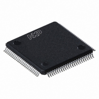
PCF2113DH/4,557 NXP Semiconductors, PCF2113DH/4,557 Datasheet - Page 38

PCF2113DH/4,557
Manufacturer Part Number
PCF2113DH/4,557
Description
IC LCD CONTROLLER/DRIVER 100LQFP
Manufacturer
NXP Semiconductors
Datasheet
1.PCF2113DH4557.pdf
(65 pages)
Specifications of PCF2113DH/4,557
Package / Case
100-LQFP
Display Type
LCD
Configuration
5 X 8 (Matrix)
Interface
I²C
Voltage - Supply
2.2 V ~ 4 V
Operating Temperature
-40°C ~ 85°C
Mounting Type
Surface Mount
Number Of Digits
40
Maximum Clock Frequency
450 KHz
Operating Supply Voltage
1.8 V to 5.5 V
Maximum Power Dissipation
400 mW
Maximum Operating Temperature
+ 75 C
Attached Touch Screen
No
Maximum Supply Current
50 mA
Minimum Operating Temperature
- 20 C
Operating Supply Voltage (typ)
2.5/3.3/5V
Package Type
LQFP
Pin Count
100
Mounting
Surface Mount
Power Dissipation
400mW
Operating Supply Voltage (min)
1.8V
Operating Supply Voltage (max)
5.5V
Lead Free Status / RoHS Status
Lead free / RoHS Compliant
Current - Supply
-
Digits Or Characters
-
Lead Free Status / Rohs Status
Lead free / RoHS Compliant
Other names
935276328557
PCF2113DH/4
PCF2113DH/4
PCF2113DH/4
PCF2113DH/4
Available stocks
Company
Part Number
Manufacturer
Quantity
Price
Company:
Part Number:
PCF2113DH/4,557
Manufacturer:
NXP Semiconductors
Quantity:
10 000
NXP Semiconductors
PCF2113_FAM_4
Product data sheet
Fig 25. Master transmits to slave receiver; write mode
S
0 1 1 1 0 1
0 1 1 1 0 1
slave address
slave address
PCF2113x
11.2.1 I
acknowledgement
from PCF2113x
S
A
S
A
0
0
R/W
R/W
0 A
0
Also a master receiver must generate an acknowledge after the reception of each byte
that has been clocked out of the slave transmitter.
The device that acknowledges must pull-down the SDA line during the acknowledge clock
pulse, so that the SDA line is stable LOW during the HIGH period of the acknowledge
related clock pulse (set-up and hold times must be taken into consideration).
A master receiver must signal an end of data to the transmitter by not generating an
acknowledge bit on the last byte that has been clocked out of the slave. In this event the
transmitter must leave the data line HIGH to enable the master to generate a STOP
condition.
Before any data is transmitted on the I
addressed first. The addressing is always carried out with the first byte transmitted after
the START procedure. The I
write cycles is shown in
I
PCF2113x.
2
2
C-bus protocol (receiver holds SCL LOW during internal operations) is not used in the
C-bus protocol
Co
1
RS
CONTROL BYTE A
2n
0 bytes
Rev. 04 — 4 March 2008
Figure
DATA BYTE
2
C-bus configuration for the different PCF2113x read and
25,
Figure 26
2
C-bus, the device which should respond is
A
Co
0
RS
and
CONTROL BYTE A
Figure
1 byte
27. The slow-down feature of the
LCD controllers/drivers
DATA BYTE
PCF2113x
n
© NXP B.V. 2008. All rights reserved.
0 bytes
data pointer
A
update
mgg002
38 of 65
P


