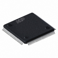
PCF2113DH/4,557 NXP Semiconductors, PCF2113DH/4,557 Datasheet - Page 45

PCF2113DH/4,557
Manufacturer Part Number
PCF2113DH/4,557
Description
IC LCD CONTROLLER/DRIVER 100LQFP
Manufacturer
NXP Semiconductors
Datasheet
1.PCF2113DH4557.pdf
(65 pages)
Specifications of PCF2113DH/4,557
Package / Case
100-LQFP
Display Type
LCD
Configuration
5 X 8 (Matrix)
Interface
I²C
Voltage - Supply
2.2 V ~ 4 V
Operating Temperature
-40°C ~ 85°C
Mounting Type
Surface Mount
Number Of Digits
40
Maximum Clock Frequency
450 KHz
Operating Supply Voltage
1.8 V to 5.5 V
Maximum Power Dissipation
400 mW
Maximum Operating Temperature
+ 75 C
Attached Touch Screen
No
Maximum Supply Current
50 mA
Minimum Operating Temperature
- 20 C
Operating Supply Voltage (typ)
2.5/3.3/5V
Package Type
LQFP
Pin Count
100
Mounting
Surface Mount
Power Dissipation
400mW
Operating Supply Voltage (min)
1.8V
Operating Supply Voltage (max)
5.5V
Lead Free Status / RoHS Status
Lead free / RoHS Compliant
Current - Supply
-
Digits Or Characters
-
Lead Free Status / Rohs Status
Lead free / RoHS Compliant
Other names
935276328557
PCF2113DH/4
PCF2113DH/4
PCF2113DH/4
PCF2113DH/4
Available stocks
Company
Part Number
Manufacturer
Quantity
Price
Company:
Part Number:
PCF2113DH/4,557
Manufacturer:
NXP Semiconductors
Quantity:
10 000
NXP Semiconductors
15. Dynamic characteristics
Table 20.
V
unless otherwise specified
PCF2113_FAM_4
Product data sheet
Symbol
f
f
f
t
t
t
Timing characteristics of parallel interface
Write operation (writing data from microcontroller to PCF2113x); see
t
t
t
t
t
t
Read operation (reading data from PCF2113x to microcontroller); see
t
t
t
t
t
t
Timing characteristics of I
f
t
t
t
t
t
t
C
t
t
fr(LCD)
osc
osc(ext)
d(startup)(OSC)
w(pd)
w(spike)
cy(en)
w(en)
su(A)
h(A)
su(D)
h(D)
cy(en)
w(en)
su(A)
h(A)
d(DV)
h(D)
SCL
LOW
HIGH
SU;DAT
HD;DAT
r
f
SU;STA
HD;STA
DD1
b
= 1.8 V to 5.5 V; V
Dynamic characteristics
Parameter
LCD frame frequency
oscillator frequency
external oscillator frequency
start-up delay time on pin OSC
power-down pulse width
spike pulse width
enable cycle time
enable pulse width
address set-up time
address hold time
data input set-up time
data input hold time
enable cycle time
enable pulse width
address set-up time
address hold time
data input valid delay time
data input hold time
SCL frequency
LOW period of the SCL clock
HIGH period of the SCL clock
data set-up time
data hold time
rise time of both SDA and SCL
signals
fall time of both SDA and SCL
signals
capacitive load for each bus line
set-up time for a repeated
START condition
hold time (repeated) START
condition
DD2
= V
2
C-bus interface
DD3
= 2.2 V to 4.0 V; V
[3]
[3]
; see
Conditions
internal clock; V
oscillator, after power down
on pin PD
V
V
Rev. 04 — 4 March 2008
DD1
DD1
SS
Figure 34
> 2.2 V
> 1.5 V
= 0 V; V
LCD
DD
= 5.0 V
= 2.2 V to 6.5 V; T
Figure 32
Figure 33
[2][4]
[2][4]
[1]
[2]
[2]
[4]
Min
45
140
140
-
1
-
500
220
50
25
60
25
500
220
50
25
-
-
5
-
1.3
0.6
100
0
15 + 0.1C
15 + 0.1C
-
0.6
0.6
amb
= 40 C to +85 C;
b
b
LCD controllers/drivers
Typ
95
250
-
200
-
-
-
-
-
-
-
-
-
-
-
-
-
-
-
-
-
-
-
-
-
-
-
-
-
PCF2113x
© NXP B.V. 2008. All rights reserved.
Max
147
450
450
300
-
90
-
-
-
-
-
-
-
-
-
-
150
250
-
400
-
-
-
-
300
300
400
-
-
Unit
Hz
kHz
kHz
ns
ns
ns
ns
ns
ns
ns
ns
ns
ns
ns
ns
ns
ns
Hz
ns
ns
ns
ns
pF
45 of 65
s
s
s
s
s
s


