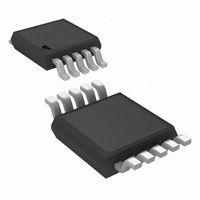
LM5069MMX-1/NOPB National Semiconductor, LM5069MMX-1/NOPB Datasheet

LM5069MMX-1/NOPB
Specifications of LM5069MMX-1/NOPB
Available stocks
Related parts for LM5069MMX-1/NOPB
LM5069MMX-1/NOPB Summary of contents
Page 1
... In-rush current limit for safe board insertion into live power sources ■ Programmable maximum power dissipation in the external pass device Typical Application © 2008 National Semiconductor Corporation ■ Adjustable current limit ■ Circuit breaker function for severe over-current events ■ Internal high side charge pump and gate driver for external N-channel MOSFET ■ ...
Page 2
... Connection Diagram Ordering Information Order Number Fault Response LM5069MM-1 Latch Off LM5069MMX-1 Latch Off LM5069MM-2 Auto Restart LM5069MMX-2 Auto Restart Pin Descriptions Pin # Name Description 1 SENSE Current sense input 2 VIN Positive supply input 3 UVLO Under-voltage lockout 4 OVLO Over-voltage lockout 5 GND Circuit ground ...
Page 3
... Absolute Maximum Ratings If Military/Aerospace specified devices are required, please contact the National Semiconductor Sales Office/ Distributors for availability and specifications. VIN to GND (Note 5) SENSE, OUT, PGD to GND GATE to GND (Note 5) UVLO to GND OVLO to GND VIN to SENSE Electrical Characteristics junction temperature (T ) range of -40°C to +125°C. Minimum and Maximum limits are guaranteed through test, design, or statistical J correlation ...
Page 4
... Note 3: OUT bias current (disabled) due to leakage current through an internal 1.0 MΩ resistance from SENSE to VOUT. Note 4: For detailed information on soldering plastic MSOP packages refer to the Packaging Databook available from National Semiconductor Corporation. Note 5: The GATE pin voltage is typically 12V above VIN when the LM5069 is enabled. Therefore the Absolute Maximum Ratings for VIN (100V) applies only when the LM5069 is disabled, or for a momentary surge to that voltage since the Absolute Maximum Rating for the GATE pin is also 100V ...
Page 5
Typical Performance Characteristics 25° 48V IN VIN Pin Input Current vs. VIN OUT Pin Current GATE Pin Source Current vs. V Unless otherwise specified the following conditions apply: T SENSE Pin Input Current 20197203 GATE Pin Voltage vs. ...
Page 6
MOSFET Power Dissipation Limit vs. R UVLO Hysteresis Current vs. Temperature UVLO, OVLO Threshold vs. Temperature www.national.com and R GATE Pull-Down Current, Circuit Breaker vs GATE Voltage PWR S 20197209 OVLO Hysteresis Current vs. Temperature 20197255 Input Current, Enabled vs. ...
Page 7
Current Limit Threshold vs. Temperature Power Limit Threshold vs. Temperature GATE Source Current vs. Temperature Circuit Breaker Threshold vs. Temperature 20197259 GATE Output Voltage vs. Temperature 20197261 GATE Pull-Down Current, Circuit Breaker vs. Temperature 20197263 7 20197260 20197262 20197264 www.national.com ...
Page 8
PGD Low Voltage vs. Temperature Block Diagram www.national.com 20197265 8 20197210 ...
Page 9
Functional Description The LM5069 is designed to control the in-rush current to the load upon insertion of a circuit card into a live backplane or other "hot" power source, thereby limiting the voltage sag on the backplane’s supply voltage, and ...
Page 10
Figure 3) an internal 85 µA fault timer current source charges Q1’s power dissipation and the T input current reduce below their respective limiting thresholds before the TIMER pin reaches 4.0V the 85 ...
Page 11
Current Limit The current limit threshold is reached when the voltage across the sense resistor R (VIN to SENSE) reaches 55 mV. In the S current limiting condition, the GATE voltage is controlled to limit the current in MOSFET Q1. ...
Page 12
The LM5069-2 provides an automatic restart sequence which consists of the TIMER pin cycling between 4.0V and 1.25V seven times after the Fault Timeout Period, as shown in Fig- ure 6. The period of each cycle is determined by the ...
Page 13
FIGURE 7. Shutdown Control Power Good Pin The Power Good indicator pin (PGD) is connected to the drain of an internal N-channel MOSFET capable of sustaining 80V in the off-state, and transients up to 100V. An external pull-up resistor is ...
Page 14
Q1’s power from exceeding the threshold. For proper operation of the power ≤ limiting feature, R must be 150 kΩ. While the power lim- PWR iting circuit is active, the fault timer is ...
Page 15
MOSFET SELECTION It is recommended that the external MOSFET (Q1) selection be based on the following criteria: - The BV rating should be greater than the maximum DSS system voltage (V ), plus ringing and transients which can SYS occur ...
Page 16
For example 0.33 µ RESTART end of the restart time switched on. If the fault is still present, the fault timeout and restart sequence repeats. The ...
Page 17
Choose the upper and lower UVLO thresholds ( UVL -Choose the upper and lower OVLO threshold ( OVL As an example, assume the application requires the following thresholds 22V 17V, V ...
Page 18
If a delay is required at PGD, suggested circuits are shown in Figure 16. In Figure 16a, capacitor C ing edge, but not to the falling edge. In Figure 16b, the rising edge is delayed and ...
Page 19
The board’s edge connector can be designed to shut off the LM5069 as the board is removed, before the supply voltage is disconnected from the LM5069. In Figure 17 the voltage at the UVLO pin goes to ground before ...
Page 20
Physical Dimensions www.national.com inches (millimeters) unless otherwise noted NS Package Number MUB10A 20 ...
Page 21
Notes 21 www.national.com ...
Page 22
... For more National Semiconductor product information and proven design tools, visit the following Web sites at: Products Amplifiers www.national.com/amplifiers Audio www.national.com/audio Clock Conditioners www.national.com/timing Data Converters www.national.com/adc Displays www.national.com/displays Ethernet www.national.com/ethernet Interface www.national.com/interface LVDS www.national.com/lvds Power Management www.national.com/power Switching Regulators www.national.com/switchers LDOs www ...


