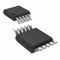
LM5069MMX-1/NOPB National Semiconductor, LM5069MMX-1/NOPB Datasheet - Page 17

LM5069MMX-1/NOPB
Manufacturer Part Number
LM5069MMX-1/NOPB
Description
IC CTLR HOT SWAP 48V 10-MSOP
Manufacturer
National Semiconductor
Type
Hot-Swap Controllerr
Datasheet
1.LM5069MMX-1NOPB.pdf
(22 pages)
Specifications of LM5069MMX-1/NOPB
Applications
General Purpose
Internal Switch(s)
No
Voltage - Supply
9 V ~ 80 V
Operating Temperature
-40°C ~ 125°C
Mounting Type
Surface Mount
Package / Case
10-TFSOP, 10-MSOP (0.118", 3.00mm Width)
For Use With
LM5069EVAL - BOARD EVALUATION LM5069
Lead Free Status / RoHS Status
Lead free / RoHS Compliant
Other names
LM5069MMX-1
Available stocks
Company
Part Number
Manufacturer
Quantity
Price
Part Number:
LM5069MMX-1/NOPB
Manufacturer:
TI/德州仪器
Quantity:
20 000
(V
(V
As an example, assume the application requires the following
thresholds: V
58V. Therefore V
values are:
R1 = 238 kΩ, R2 = 41 kΩ
R3 = 95.2 kΩ, R4 = 4.14 kΩ
Where the R1-R4 resistor values are known, the threshold
voltages and hysteresis are calculated from the following:
Option D: The OVLO function can be disabled by grounding
the OVLO pin. The UVLO thresholds are set as described in
Option B or Option C.
POWER GOOD PIN
During turn-on, the Power Good pin (PGD) is high until the
voltage at VIN increases above
- Choose the upper and lower UVLO thresholds (V
UVL
-Choose the upper and lower OVLO threshold (V
OVL
).
).
UVH
UV(HYS)
= 22V, V
= 5V, and V
UVL
= 17V, V
≊
FIGURE 14. UVLO = POR
5V. PGD then switches low,
OV(HYS)
OVH
= 60V, and V
= 2V. The resistor
OVH
UVH
) and
OVL
) and
=
EN
with Shutdown/Restart Control
17
Option C: The minimum UVLO level is obtained by connect-
ing the UVLO pin to VIN as shown in Figure 14. Q1 is switched
on when the VIN voltage reaches the POR
(
provide remote shutdown control, and to restart the LM5069-1
after a fault detection. The OVLO thresholds are set using R3,
R4. Their values are calculated using the procedure in Option
B.
remaining low as the VIN voltage increases. When the voltage
at OUT increases to within 1.25V of the SENSE pin (V
<1.25V), PGD switches high. PGD switches low if the V
Q1 increases above 2.5V. A pull-up resistor is required at
PGD as shown in Figure 15. The pull-up voltage (V
be as high as 80V, with transient capability to 100V, and can
be higher or lower than the voltages at VIN and OUT.
≊
8.4V). An external transistor can be connected to UVLO to
V
V
UV(HYS)
OV(HYS)
= R1 x 21 µA
= R3 x 21 µA
20197250
EN
www.national.com
threshold
PGD
) can
DS
DS
of


