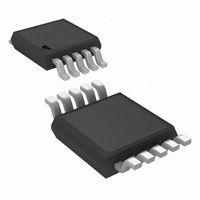
LM5069MMX-1/NOPB National Semiconductor, LM5069MMX-1/NOPB Datasheet - Page 13

LM5069MMX-1/NOPB
Manufacturer Part Number
LM5069MMX-1/NOPB
Description
IC CTLR HOT SWAP 48V 10-MSOP
Manufacturer
National Semiconductor
Type
Hot-Swap Controllerr
Datasheet
1.LM5069MMX-1NOPB.pdf
(22 pages)
Specifications of LM5069MMX-1/NOPB
Applications
General Purpose
Internal Switch(s)
No
Voltage - Supply
9 V ~ 80 V
Operating Temperature
-40°C ~ 125°C
Mounting Type
Surface Mount
Package / Case
10-TFSOP, 10-MSOP (0.118", 3.00mm Width)
For Use With
LM5069EVAL - BOARD EVALUATION LM5069
Lead Free Status / RoHS Status
Lead free / RoHS Compliant
Other names
LM5069MMX-1
Available stocks
Company
Part Number
Manufacturer
Quantity
Price
Part Number:
LM5069MMX-1/NOPB
Manufacturer:
TI/德州仪器
Quantity:
20 000
Power Good Pin
The Power Good indicator pin (PGD) is connected to the drain
of an internal N-channel MOSFET capable of sustaining 80V
in the off-state, and transients up to 100V. An external pull-up
resistor is required at PGD to an appropriate voltage to indi-
cate the status to downstream circuitry. The off-state voltage
at the PGD pin can be higher or lower than the voltages at
VIN and OUT. PGD is switched high when the voltage from
SENSE to OUT (the external MOSFET’s V
low 1.25V. PGD switches low when the MOSFET’s V
increased past 2.5V. If the UVLO pin is taken below 2.5V, or
the OVLO pin taken above 2.5V, to disable the LM5069, PGD
switches low within 10 µs without waiting for the voltage at
OUT to fall 2.5V below the voltage at SENSE. The PGD output
pin is high when the voltage at VIN is less than 5V.
Application Information
(Refer to Figure 1)
CURRENT LIMIT, R
The LM5069 monitors the current in the external MOSFET
(Q1) by measuring the voltage across the sense resistor
POWER LIMIT THRESHOLD
The LM5069 determines the power dissipation in the external
MOSFET (Q1) by monitoring the drain current (the current in
R
the PWR pin (R
Q1, and is calculated from the following equation:
S
), and the V
DS
FIGURE 7. Shutdown Control
PWR
of Q1 (SENSE to OUT pins). The resistor at
) sets the maximum power dissipation for
S
DS
FIGURE 8. Sense Resistor Connections
) decreases be-
20197217
DS
is
13
(R
value is calculated from:
where I
across R
the gate of Q1 to regulate the current at I
limiting circuit is active, the fault timer is active as described
in the Fault Timer & Restart section. For proper operation,
R
While the maximum load current in normal operation can be
used to determine the required power rating for resistor R
basing it on the current limit value provides a more reliable
design since the circuit can operate near the current limit
threshold continuously. The resistor’s surge capability must
also be considered since the circuit breaker threshold is twice
the current limit threshold. Connections from R
LM5069 should be made using Kelvin techniques. In the sug-
gested layout of Figure 8 the small pads at the lower corners
of the sense resistor connect only to the sense resistor ter-
minals, and not to the traces carrying the high current. With
this technique, only the voltage across the sense resistor is
applied to VIN and SENSE, eliminating the voltage drop
across the high current solder connections.
where P
and R
Limit section. For example, if R
power limit threshold is 60W, R
power dissipation reaches the threshold Q1’s gate is modu-
S
S
must be no larger than 100 mΩ.
), connected from VIN to SENSE. The required resistor
S
LIM
is the current sense resistor described in the Current
FET(LIM)
S
R
is the desired current limit threshold. If the voltage
reaches 55 mV, the current limit circuit modulates
PWR
= 1.25 x 10
is the desired power limit threshold for Q1,
20197219
5
x R
PWR
S
S
is 10 mΩ , and the desired
x P
calculates to 75 kΩ. If Q1’s
FET(LIM)
LIM
. While the current
www.national.com
S
to the
(1)
(2)
S
,


