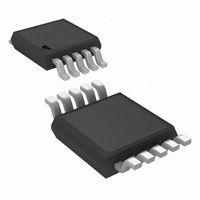
LM5069MMX-1/NOPB National Semiconductor, LM5069MMX-1/NOPB Datasheet - Page 15

LM5069MMX-1/NOPB
Manufacturer Part Number
LM5069MMX-1/NOPB
Description
IC CTLR HOT SWAP 48V 10-MSOP
Manufacturer
National Semiconductor
Type
Hot-Swap Controllerr
Datasheet
1.LM5069MMX-1NOPB.pdf
(22 pages)
Specifications of LM5069MMX-1/NOPB
Applications
General Purpose
Internal Switch(s)
No
Voltage - Supply
9 V ~ 80 V
Operating Temperature
-40°C ~ 125°C
Mounting Type
Surface Mount
Package / Case
10-TFSOP, 10-MSOP (0.118", 3.00mm Width)
For Use With
LM5069EVAL - BOARD EVALUATION LM5069
Lead Free Status / RoHS Status
Lead free / RoHS Compliant
Other names
LM5069MMX-1
Available stocks
Company
Part Number
Manufacturer
Quantity
Price
Part Number:
LM5069MMX-1/NOPB
Manufacturer:
TI/德州仪器
Quantity:
20 000
MOSFET SELECTION
It is recommended that the external MOSFET (Q1) selection
be based on the following criteria:
-
system voltage (V
occur at V
inserted or removed.
-
on the current limit threshold (55 mV/R
load current, since the circuit can operate near the current
limit threshold continuously.
-
the current threshold for the circuit breaker function (105 mV/
R
-
the thermal properties, should be used to determine the max-
imum power dissipation threshold set by the R
The programmed maximum power dissipation should have a
reasonable margin from the maximum power defined by the
FET's SOA chart if the LM5069-2 is used since the FET will
be repeatedly stressed during fault restart cycles. The FET
manufacturer should be consulted for guidelines.
-
tion at maximum load current (I
its junction temperature above the manufacturer’s recom-
mendation.
If the device chosen for Q1 has a maximum V
than 12V, an external zener diode must be added from its gate
to source, with the zener voltage less than the maximum
V
at least 250 mA to conduct the GATE pull-down current during
startup and in the circuit breaker mode.
TIMER CAPACITOR, C
The TIMER pin capacitor (C
time delay, fault timeout period, and restart timing of the
LM5069-2.
A) Insertion Delay - Upon applying the system voltage
(V
during the insertion time (t1 in Figure 3) to allow ringing and
transients at V
to a circuit card plug-in is unique, the worst case settling time
GS
S
SYS
).
The Pulsed Drain Current spec (I
The maximum continuous current rating should be based
The SOA (Safe Operating Area) chart of the device, and
The BV
R
rating. The zener diode’s forward current rating must be
DS(on)
) to the circuit, the external MOSFET (Q1) is held off
SYS
should be sufficiently low that the power dissipa-
DSS
SYS
when the circuit card, or adjacent cards, are
rating should be greater than the maximum
SYS
to settle. Since each backplane’s response
), plus ringing and transients which can
T
T
) sets the timing for the insertion
L(max)
2
DM
x R
) must be greater than
S
DS(on)
), not the maximum
FIGURE 11. MOSFET Power Up Waveforms
) does not raise
GS
PWR
rating less
resistor.
15
must be determined for each application. The insertion time
starts when VIN reaches the POR
the internal 5.5 µA current source charges C
The required capacitor value is calculated from:
For example, if the desired insertion delay is 250 ms, C
culates to 0.345 µF. At the end of the insertion delay, C
quickly discharged by a 1.5 mA current sink.
B) Fault Timeout Period - During in-rush current limiting or
upon detection of a fault condition where the current limit and/
or power limit circuits regulate the current through Q1, the
fault timer current source (85 µA) is switched on to charge
C
TIMER pin voltage to reach 4.0V, at which time Q1 is switched
off. The required capacitor value for the desired Fault Timeout
Period t
For example, if the desired Fault Timeout Period is 16 ms,
C
LM5069-1 latches the GATE pin low until a power up se-
quence is initiated by external circuitry. C
the 2.5 µA current sink at the end of the Fault Timeout Period.
See the Fault Timer and Restart section and Figure 5. When
the Fault Timeout Period of the LM5069-2 expires, a restart
sequence starts as described below (Restart Timing). Since
the LM5069 normally operates in power limit and/or current
limit during a power up sequence, the Fault Timeout Period
must be longer than the time required for the output voltage
to reach its final value. See the Turn-on Time section.
C) Restart Timing For the LM5069-2, after the Fault Timeout
Period described above, C
rent sink to 1.25V. The TIMER pin then cycles through seven
additional charge/discharge cycles between 1.25V and 4.0V
as shown in Figure 6. The restart time ends when the TIMER
pin voltage reaches 0.3V during the final high-to-low ramp.
The restart time, after the Fault Timeout Period, is equal to:
T
T
. The Fault Timeout Period is the time required for the
calculates to 0.34 µF. After the Fault Timeout Period, the
FAULT
is calculated from:
T
is discharged by the 2.5 µA cur-
IT
threshold, at which time
T
T
is discharged by
20197225
from 0V to 4.0V.
www.national.com
T
cal-
T
(3)
is


