LM5069MMX-1/NOPB National Semiconductor, LM5069MMX-1/NOPB Datasheet - Page 12
LM5069MMX-1/NOPB
Manufacturer Part Number
LM5069MMX-1/NOPB
Description
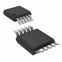
IC CTLR HOT SWAP 48V 10-MSOP
Manufacturer
National Semiconductor
Type
Hot-Swap Controllerr
Datasheet
1.LM5069MMX-1NOPB.pdf
(22 pages)
Specifications of LM5069MMX-1/NOPB
Applications
General Purpose
Internal Switch(s)
No
Voltage - Supply
9 V ~ 80 V
Operating Temperature
-40°C ~ 125°C
Mounting Type
Surface Mount
Package / Case
10-TFSOP, 10-MSOP (0.118", 3.00mm Width)
For Use With
LM5069EVAL - BOARD EVALUATION LM5069
Lead Free Status / RoHS Status
Lead free / RoHS Compliant
Other names
LM5069MMX-1
Available stocks
Company
Part Number
Manufacturer
Quantity
Price

Part Number:
LM5069MMX-1/NOPB
Manufacturer:
TI/德州仪器
Quantity:
20 000


www.national.com
The LM5069-2 provides an automatic restart sequence which
consists of the TIMER pin cycling between 4.0V and 1.25V
seven times after the Fault Timeout Period, as shown in Fig-
ure 6. The period of each cycle is determined by the 85 µA
charging current, and the 2.5 µA discharge current, and the
Under-Voltage Lock-Out (UVLO)
The series pass MOSFET (Q1) is enabled when the input
supply voltage (V
the programmable under-voltage lockout (UVLO) and over-
voltage lock-out (OVLO) levels. Typically the UVLO level at
V
1. When V
current source at UVLO is enabled, the current source at OV-
LO is off, and Q1 is held off by the 2 mA pull-down current at
the GATE pin. As V
UVLO above 2.5V, the 21 µA current source at UVLO is
switched off, increasing the voltage at UVLO, providing hys-
teresis for this threshold. With the UVLO pin above 2.5V, Q1
is switched on by the 16 µA current source at the GATE pin if
the insertion time delay has expired (Figure 3). See the Ap-
plications Section for a procedure to calculate the values of
the threshold setting resistors (R1-R3). The minimum possi-
ble UVLO level at V
pin to VIN. In this case Q1 is enabled when the VIN voltage
reaches the POR
SYS
is set with a resistor divider (R1-R3) as shown in Figure
SYS
is below the UVLO level, the internal 21 µA
SYS
EN
SYS
) is within the operating range defined by
threshold.
SYS
can be set by connecting the UVLO
is increased, raising the voltage at
FIGURE 5. Latched Fault Restart Control
FIGURE 6. Restart Sequence (LM5069-2)
12
value of the capacitor C
during the eighth high-to-low ramp, the 16 µA current source
at the GATE pin turns on Q1. If the fault condition is still
present, the Fault Timeout Period and the restart cycle repeat.
Over-Voltage Lock-Out (OVLO)
The series pass MOSFET (Q1) is enabled when the input
supply voltage (V
the programmable under-voltage lockout (UVLO) and over-
voltage lock-out (OVLO) levels. If V
voltage above 2.5V Q1 is switched off by the 2 mA pull-down
current at the GATE pin, denying power to the load. When the
OVLO pin is above 2.5V, the internal 21 µA current source at
OVLO is switched on, raising the voltage at OVLO to provide
threshold hysteresis. When V
level Q1 is enabled. See the Applications Section for a pro-
cedure to calculate the threshold setting resistor values.
Shutdown Control
The load current can be remotely switched off by taking the
UVLO pin below its 2.5V threshold with an open collector or
open drain device, as shown in Figure 7. Upon releasing the
UVLO pin the LM5069 switches on the load current with in-
rush current and power limiting.
20197215
SYS
) is within the operating range defined by
T
. When the TIMER pin reaches 0.3V
SYS
is reduced below the OVLO
SYS
20197216
raises the OVLO pin
Related parts for LM5069MMX-1/NOPB
Image
Part Number
Description
Manufacturer
Datasheet
Request
R

Part Number:
Description:
IC CTLR HOT SWAP 48V 10-MSOP
Manufacturer:
National Semiconductor
Datasheet:

Part Number:
Description:
IC,Power Control/Management,TSSOP,10PIN,PLASTIC
Manufacturer:
National Semiconductor
Part Number:
Description:
IC,Power Control/Management,TSSOP,10PIN,PLASTIC
Manufacturer:
National Semiconductor
Part Number:
Description:
National Semiconductor [8-Bit D/A Converter]
Manufacturer:
National Semiconductor
Datasheet:
Part Number:
Description:
National Semiconductor [Media Coprocessor]
Manufacturer:
National Semiconductor
Datasheet:
Part Number:
Description:
Digitally Controlled Tone and Volume Circuit with Stereo Audio Power Amplifier, Microphone Preamp Stage and National 3D Sound
Manufacturer:
National Semiconductor
Datasheet:
Part Number:
Description:
Digitally Controlled Tone and Volume Circuit with Stereo Audio Power Amplifier, Microphone Preamp Stage and National 3D Sound
Manufacturer:
National Semiconductor
Datasheet:
Part Number:
Description:
AC97 Rev 2 Codec with Sample Rate Conversion and National 3D Sound
Manufacturer:
National Semiconductor
Part Number:
Description:
Manufacturer:
National Semiconductor
Datasheet:
Part Number:
Description:
Manufacturer:
National Semiconductor
Datasheet:
Part Number:
Description:
General Purpose, Low Voltage, Low Power, Rail-to-Rail Output Operational Amplifiers
Manufacturer:
National Semiconductor
Datasheet:
Part Number:
Description:
8-bit 20 MSPS flash A/D converter.
Manufacturer:
National Semiconductor
Datasheet:
Part Number:
Description:
Low Noise Quad Operational Amplifier
Manufacturer:
National Semiconductor
Datasheet:
Part Number:
Description:
Quad Differential Line Receivers
Manufacturer:
National Semiconductor
Datasheet: