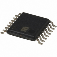
MIC2584-JBTS Micrel Inc, MIC2584-JBTS Datasheet - Page 20

MIC2584-JBTS
Manufacturer Part Number
MIC2584-JBTS
Description
IC CTRLR HOT SWAP DUAL 16-TSSOP
Manufacturer
Micrel Inc
Type
Hot-Swap Controllerr
Datasheet
1.MIC2584-JYTS.pdf
(28 pages)
Specifications of MIC2584-JBTS
Applications
General Purpose
Internal Switch(s)
No
Voltage - Supply
1 V ~ 13.2 V
Operating Temperature
-40°C ~ 85°C
Mounting Type
Surface Mount
Package / Case
16-TSSOP
Linear Misc Type
Positive Low Voltage
Family Name
MIC2584
Package Type
TSSOP
Operating Supply Voltage (min)
1V
Operating Supply Voltage (max)
13.2V
Operating Temperature (min)
-40C
Operating Temperature (max)
85C
Operating Temperature Classification
Industrial
Product Depth (mm)
4.4mm
Product Height (mm)
0.9mm
Product Length (mm)
5mm
Mounting
Surface Mount
Pin Count
16
Lead Free Status / RoHS Status
Contains lead / RoHS non-compliant
Available stocks
Company
Part Number
Manufacturer
Quantity
Price
Company:
Part Number:
MIC2584-JBTS
Manufacturer:
MIC
Quantity:
23
Company:
Part Number:
MIC2584-JBTS
Manufacturer:
MICREL
Quantity:
240
Part Number:
MIC2584-JBTS
Manufacturer:
MICREL/麦瑞
Quantity:
20 000
MIC2584/2585
Output Undervoltage Detection
For output undervoltage detection, the first consideration is to
establish the output voltage level that indicates “power is
good.” For this example, the output value for which a 12V
supply will signal “good” is 10.5V. Next, consider the toler-
ances of the input supply and FB threshold (V
example, given a 12V 5% supply for Channel 1, the resulting
output voltage may be as low as 11.4V and as high as 12.6V.
Additionally, the FB1 threshold has 50mV tolerance and
may be as low as 1.19V and as high as 1.29V. Thus, to
determine the values of the resistive divider network (R12
and R13) at the FB1 pin, shown in the typical application
circuit on page 1, use the following iterative design proce-
dure.
MIC2584/2585
1) Choose R13 so as to limit the current through
R13 is chosen as 14.7k
R13
the divider to approximately 100 A or less.
3.3V
V
V
5V
IN1
IN2
V
FB1(MAX)
100 A
Undervoltage (OUT1) = 4.4V
Undervoltage (OUT2) = 2.85V
Circuit Breaker Response Time = 5ms
Sequenced Output Delay (Turn-On) = 20ms
*Dual package Diode is AZ23C8V2
Resistors are 5% unless specified otherwise
Additional pins omitted for clarity
0.01 F
R1
33k
R2
47k
(8V)
(8V)
*D1
*D2
C5
0.1 F
C6
100 A
1.29V
11
12
C1
1 F
C2
1 F
8
CFILTER
CDLY
ON
1%.
VCC1
12.9k
3
Figure 8. First On—Last Off Application Circuit
24
1
R
0.012
SENSE1
5%
SENSE1
.
2
4
23
MIC2585-1
GND
FB
13
VCC2
). For this
3
1
1
R
0.012
SENSE2
5%
TRK
SENSE2
9
2
GATE2
GATE1
4
OUT2
OUT1
2
20
DIS2
DIS1
FB2
FB1
Using some basic algebra and simplifying Equation 10 to
isolate R12, yields:
where V
14.7k . Substituting these values into Equation 10.1 now
yields R12 = 104.95k . A standard 105k
Now, consider the 11.4V minimum output voltage, the lower
tolerance for R13 and higher tolerance for R12, 14.55k and
106.05k , respectively. With only 11.4V available, the voltage
sensed at the FB1 pin exceeds V
PG1 (MIC2585) signals will transition from LOW to HIGH,
indicating “power is good” given the worse case tolerances of
this example. A similar approach should be used for Channel 2.
IRF7822
(SO-8)
3
7
5
6
22
19
20
18
0.033 F
Q2
2) Next, determine R12 using the output “good”
R8
1.5k
C7
R12 R13
V
R9
3.6k
voltage of 10.5V and the following equation:
R7
680
OUT1(Good)
FB1(MAX)
R5
20.5k
1%
C4
0.022 F
R6
8.66k
1%
0.022 F
IRF7822
C3
(SO-8)
= 1.29V, V
Q1
V
V
OUT1(Good)
V
FB1(MAX)
FB1(MAX)
OUT1(Good)
ZTX788A
TCR22-4
R3
39.2k
1%
R4
15.8k
1%
360
R10
FB1(MAX)
Q4
Q3
R12 R13
– 1
C
220 F
R13
LOAD1
C
220 F
LOAD2
= 10.5V, and R13 is
, thus the /POR and
V
5V@2.5A
V
3.3V@2.5A
OUT1
OUT2
1% is selected.
March 2005
(10)
(10.1)
Micrel


