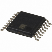
MIC2584-JBTS Micrel Inc, MIC2584-JBTS Datasheet - Page 4

MIC2584-JBTS
Manufacturer Part Number
MIC2584-JBTS
Description
IC CTRLR HOT SWAP DUAL 16-TSSOP
Manufacturer
Micrel Inc
Type
Hot-Swap Controllerr
Datasheet
1.MIC2584-JYTS.pdf
(28 pages)
Specifications of MIC2584-JBTS
Applications
General Purpose
Internal Switch(s)
No
Voltage - Supply
1 V ~ 13.2 V
Operating Temperature
-40°C ~ 85°C
Mounting Type
Surface Mount
Package / Case
16-TSSOP
Linear Misc Type
Positive Low Voltage
Family Name
MIC2584
Package Type
TSSOP
Operating Supply Voltage (min)
1V
Operating Supply Voltage (max)
13.2V
Operating Temperature (min)
-40C
Operating Temperature (max)
85C
Operating Temperature Classification
Industrial
Product Depth (mm)
4.4mm
Product Height (mm)
0.9mm
Product Length (mm)
5mm
Mounting
Surface Mount
Pin Count
16
Lead Free Status / RoHS Status
Contains lead / RoHS non-compliant
Available stocks
Company
Part Number
Manufacturer
Quantity
Price
Company:
Part Number:
MIC2584-JBTS
Manufacturer:
MIC
Quantity:
23
Company:
Part Number:
MIC2584-JBTS
Manufacturer:
MICREL
Quantity:
240
Part Number:
MIC2584-JBTS
Manufacturer:
MICREL/麦瑞
Quantity:
20 000
MIC2584/2585
MIC2584/2585
Pin Number
MIC2584
3, 14
5, 12
4, 13
N/A
N/A
10
11
9
7
8
Pin Number
MIC2585
3, 22
7, 18
5, 20
13
10
11
14
15
12
9
GATE2, GATE1
OUT2, OUT1
Pin Name
CFILTER
FB2, FB1
/FAULT
CPOR
CDLY
/POR
GND
TRK
Pin Function
Gate Drive (Outputs): Connect each output to the gates of external
N-Channel MOSFETs. When ON is asserted, a 14 A current source is
activated and begins to charge the gate of the N-Channel MOSFET connected
to this pin. An internal clamp ensures that no more than 10V is applied
between the GATE and Source when VCC1 or VCC2 is above 5V. When the
circuit breaker trips or when an input undervoltage lockout condition is
detected, the GATE1 and GATE2 pins are immediately brought low.
Ground: Tie to analog ground.
Power-On Reset Timer (Input): A capacitor connected between this pin and
ground sets the start-up delay (t
(t
asserts, the capacitor connected to CPOR begins to charge. When the
voltage at CPOR crosses 0.3V, the start-up threshold (V
is initiated as the GATE outputs begin to ramp while capacitor C
immediately discharged to ground. When the voltage at the lagging FB pin
rises above its threshold (V
When the voltage at CPOR rises above the power-on reset delay threshold
(V
deasserted. If C
Current Limit Response Timer (Input): A capacitor connected to this pin
defines the period of time, t
to signal a fault condition and trip the circuit breaker. When an overcurrent
condition occurs, a 2.5 A current source begins to charge this capacitor. If
the voltage at this pin reaches 1.235V, the circuit breaker is tripped, both
GATE pins immediately shut off, and /FAULT is asserted. If C
then t
Power-Good Threshold Input (Undervoltage Detect): FB1 and FB2 are
internally compared to 1.235V and 0.80V references with 25mV of hyster-
esis, respectively. External resistive divider networks may be used to set the
voltage at these pins. If either FB input momentarily goes below its thresh-
old, then /POR is activated for one timing cycle, t
undervoltage condition. The /POR signal deasserts one timing cycle after the
FB pin exceeds its power-good threshold by 25mV. A 5 s filter on these pins
prevents glitches from inadvertently activating the /POR signal.
Circuit Breaker Fault Status (Output): Active-Low, weak pull-up to VCC1 or
open-drain. Asserted when the circuit breaker is tripped due to an
overcurrent, undervoltage lockout, or overvoltage event. When deasserted,
the MIC2585 will initiate a new start cycle by toggling the ON pin.
Power-On Reset (Output): Active Low, weak pull-up to VCC1 or open drain.
This pin remains asserted during start-up until a time period (t
lagging FB pin threshold (V
C
falls below V
Output Voltage Monitor (Inputs): For output tracking, connect these pins to
their respective output to sense the output voltage.
Output Sequence Delay Timer (Input): This pin is internally clamped to 6V.
A capacitor connected to this pin sets a timer delay, t
and V
resistor, and if C
with the same dv/dt as depicted in the Tracking Mode diagram while
maintaining a maximum voltage differential between V
Discharge Tracking Mode Pin (Input): Tie this pin to OUT1 or OUT2 to
enable tracking during turn-off cycle. Ground this pin to disable tracking
during turn-off. The TRK pin is not to be used as a digital input.
POR
POR
POR
). Once the lagging supply rises above its UVLO threshold and ON
OCSLOW
OUT2
) of 1.235V, the timer resets by pulling CPOR to ground and /POR is
determines t
4
as shown in Figure 5. With this pin pulled up to VCC1 through a
FB
defaults to 20 s.
, /POR is asserted for a minimum of one timing cycle (t
POR
GATE1
POR
= 0, then t
. When the output voltage monitored at either FB pin
= C
GATE2
FB
OCSLOW
FB1
), capacitor CPOR begins to charge again.
START
or V
START
, both V
, in which an overcurrent event must last
FB2
defaults to 20 s.
) and the power-on reset interval
) is exceeded. The timing capacitor
OUT1
and V
POR
OUT2
, indicating an output
DLY
OUT1
START
, between V
ramp up and down
and V
FILTER
POR
), a start cycle
POR
) after the
OUT2
March 2005
= 0,
OUT1
is
POR
.
Micrel
).


