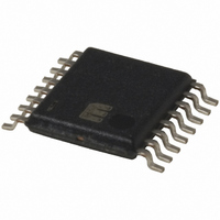
MIC2584-JBTS Micrel Inc, MIC2584-JBTS Datasheet - Page 21

MIC2584-JBTS
Manufacturer Part Number
MIC2584-JBTS
Description
IC CTRLR HOT SWAP DUAL 16-TSSOP
Manufacturer
Micrel Inc
Type
Hot-Swap Controllerr
Datasheet
1.MIC2584-JYTS.pdf
(28 pages)
Specifications of MIC2584-JBTS
Applications
General Purpose
Internal Switch(s)
No
Voltage - Supply
1 V ~ 13.2 V
Operating Temperature
-40°C ~ 85°C
Mounting Type
Surface Mount
Package / Case
16-TSSOP
Linear Misc Type
Positive Low Voltage
Family Name
MIC2584
Package Type
TSSOP
Operating Supply Voltage (min)
1V
Operating Supply Voltage (max)
13.2V
Operating Temperature (min)
-40C
Operating Temperature (max)
85C
Operating Temperature Classification
Industrial
Product Depth (mm)
4.4mm
Product Height (mm)
0.9mm
Product Length (mm)
5mm
Mounting
Surface Mount
Pin Count
16
Lead Free Status / RoHS Status
Contains lead / RoHS non-compliant
Available stocks
Company
Part Number
Manufacturer
Quantity
Price
Company:
Part Number:
MIC2584-JBTS
Manufacturer:
MIC
Quantity:
23
Company:
Part Number:
MIC2584-JBTS
Manufacturer:
MICREL
Quantity:
240
Part Number:
MIC2584-JBTS
Manufacturer:
MICREL/麦瑞
Quantity:
20 000
Input Overvoltage Protection
A similar design approach as the previous Undervoltage
Detection example is recommended for the overvoltage
protection circuitry, resistors R6 and R7 for OV1, in Figure 1.
For input overvoltage protection, the first consideration is to
establish the input voltage level that indicates an overvoltage
triggering a system (output voltage) shut down. For our
example, the input value for which the Channel 1 12V supply
will signal an “output shutdown” is 13.2V (+10%). Similarly,
from the previous example:
Now, consider the 12.6V maximum input voltage
(V
for R6, 13.13k and 128.7k , respectively. With 12.6V input,
March 2005
MIC2584/2585
/ON_OFF
CC1
/FAULT
1) Choose R7 to satisfy 100 A condition.
2) Thus, following the previous example and
GND
V
+5%), the higher tolerance for R7 and lower tolerance
R7 is chosen as 13.0k
substituting R6 and R7 for R12 and R13,
respectively, V
overvoltage for 10.5V output “good,” the same
formula yields R6 of 131.2k . The nearest
standard 1% value is 130k .
5V
R7
IN1
V
Backplane
Connector
OV1(MIN)
100 A
OV1(MIN)
PCB Edge
Connector
100 A
1.19V
Medium or
Short
Short Pin
Long
Pin
Pin
for V
33k
PCB Connection Sense
Figure 9. PCB Connection Sense with ON/OFF Control
R1
33
20k
1%
Long
R3
Pin
11.9k
R4
FB1(MAX)
Undervoltage (Output) = 4.45V
/POR Delay = 16.5ms
START-UP Delay = 4ms
Circuit Breaker Response Time = 5ms
*Q2 is TN0201T (SOT-23)
Channel 2 and additional pins omitted for clarity.
*Q2
, and 13.2V
33k
R2
C1
1 F
0.033 F
10
6
C3
ON
/FAULT
CPOR
VCC1
3
16
1
7
R
0.005
SENSE1
5%
21
MIC2584
SENSE1
GND
2
the voltage sensed at the OV1 pin is below V
MIC2584/85 will not indicate an overvoltage condition until
V
tolerances. A similar approach should be used for Channel 2.
PCB Connection Sense
There are several configuration options for the MIC2584/85’s
ON pin to detect if the PCB has been fully seated in the
backplane before initiating a start-up cycle. In Figure 1, the
MIC2584/85 is mounted on the PCB with a resistive divider
network connected to the ON pin. R4 is connected to a short
pin on the PCB edge connector. Until the connectors mate,
the ON pin is held low which keeps the GATE output charge
pump off. Once the connectors mate, the resistor network is
pulled up to the input supply, 12V in this example, and the ON
pin voltage exceeds its threshold (V
MIC2584/85 initiates a start-up cycle. In Figure 9, the connec-
tion sense consisting of a discrete logic-level MOSFET
and a few resistors allows for interrupt control from the
processor or other signal controller to shut off the output of the
MIC2584/85. R4 pulls the GATE of Q2 to V
is held low until the connectors are fully mated. Once the
connectors fully mate, a logic LOW at the /ON_OFF signal
turns Q2 off and allows the ON pin to pull up above its
threshold and initiate a start-up cycle. Applying a logic HIGH
at the /ON_OFF signal will turn Q2 on and short the ON pin
of the MIC2584/85 to ground which turns off the GATE output
charge pump.
4
15
9
CC1
CFILTER
exceeds approximately 13.2V considering the given
GATE1
OUT1
/POR
8
FB1
C4
0.01 F
(PowerPAK™ SO-8)
14
13
12
11
Si7892DP
Q1
Downstream
Signal
R5
10
C2
0.01 F
ON
R6
27.4k
1%
R7
10.5k
1%
) of 1.235V and the
IN
OV1(MIN)
MIC2584/2585
and the ON pin
C
1000 F
LOAD1
, and the
5V@7A
V
OUT1
Micrel


