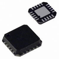
ADP5020ACPZ-R7 Analog Devices Inc, ADP5020ACPZ-R7 Datasheet - Page 20

ADP5020ACPZ-R7
Manufacturer Part Number
ADP5020ACPZ-R7
Description
IC REG LDO DUAL BUCK 20LFCSP
Manufacturer
Analog Devices Inc
Datasheet
1.ADP5020ACPZ-R7.pdf
(28 pages)
Specifications of ADP5020ACPZ-R7
Design Resources
Powering AD9272 with ADP5020 Switching Regulator PMU for Increased Efficiency (CN0135)
Applications
Handheld/Mobile Devices
Current - Supply
10mA
Voltage - Supply
2.4 V ~ 5.5 V
Operating Temperature
-40°C ~ 85°C
Mounting Type
Surface Mount
Package / Case
20-LFCSP
Supply Voltage
5.5V
No. Of Step-down Dc - Dc Converters
2
No. Of Ldo Regulators
1
Digital Ic Case Style
LFCSP
No. Of Pins
20
No. Of Regulated Outputs
3
Operating Temperature Range
-40°C To
Lead Free Status / RoHS Status
Lead free / RoHS Compliant
Other names
ADP5020ACPZ-R7TR
ADP5020
The application processor, together with the regulator power
good signal, controls the XSHTDN pin, as shown in Table 18.
After a regulator is enabled and no failure condition is detected
(power good = 1 in Bits[3:1] of the REG_CONTROL_STATUS
register, Address 0x03), the level of the XSHTDN pin is con-
trolled by Bit 0 (FORCE_XS) in the REG_CONTROL_STATUS
register. Therefore, the application processor can write to this
register to gain control over the XSHTDN pin. However, if the
EN signal is high, the level on the XSHTDN pin depends on the
power good condition of the regulator.
Table 18. Truth Table
EN
Pin
0
0
0
0
1
1
1
X = don’t care.
I
0
1
1
1
X
X
2
C Regulator Enable
1
1
OPERATION
NORMAL
END, AND ALL REGULATIONS ARE
EN = LOW AND 1
Power
Good
0
X
0
1
1
0
1
OR VDDx < V
POWER GOOD
COMMAND
SEQUENCE
VDDx < V
COMMANDS
FORCE_XS
X
0
1
1
X
X
1
1
1
UVLOF
TSD
I
2
2
C OFF
C
POR
(EN_ALL OR EN = HIGH)
XSHTDN
Pin
0
0
0
1
1
0
DEVICE ENABLED
Figure 27. State Flow
Rev. 0 | Page 20 of 28
SEQUENCER
VDDx > V
NO POWER
INTERNAL
STAND BY
EN = LOW
STARTUP
RESET
LEVEL
POR
POWER-UP/POWER-DOWN STATE FLOW
When the device is enabled, the UVLO circuit constantly monitors
the supply voltage. If the supply voltage falls below the V
threshold, typically 2.0 V, the regulators are immediately turned
off. All the internal analog circuits are then disabled to save power,
except the power-on reset (POR) circuit, which detects if the supply
voltage is dropping. If the supply voltage is higher than the POR
threshold, the POR circuit keeps the logic circuits operating
properly and retains the internal values of the registers. This
POR threshold is set to approximately 1.4 V.
If the supply voltage goes below the V
below the POR threshold, the registers are preserved. If the supply
voltage returns to the normal operating level (above V
a new activation does not require initialization of the registers.
However, if the supply voltage goes below the POR level, the
device is held in reset state. When the input voltage resumes the
proper operating level, the host controller must reload the registers.
The additional current required to keep the POR monitoring
circuits alive during UVLO is estimated to be approximately 1 μA.
EN = LOW OR I
OR VDDx < V
COMMAND
UVLOF
2
C OFF
EN = HIGH
VDD
x
UVLOR
< V
POR
threshold, but not
UVLOR
UVLOF
),


