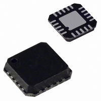
ADP5020ACPZ-R7 Analog Devices Inc, ADP5020ACPZ-R7 Datasheet - Page 9

ADP5020ACPZ-R7
Manufacturer Part Number
ADP5020ACPZ-R7
Description
IC REG LDO DUAL BUCK 20LFCSP
Manufacturer
Analog Devices Inc
Datasheet
1.ADP5020ACPZ-R7.pdf
(28 pages)
Specifications of ADP5020ACPZ-R7
Design Resources
Powering AD9272 with ADP5020 Switching Regulator PMU for Increased Efficiency (CN0135)
Applications
Handheld/Mobile Devices
Current - Supply
10mA
Voltage - Supply
2.4 V ~ 5.5 V
Operating Temperature
-40°C ~ 85°C
Mounting Type
Surface Mount
Package / Case
20-LFCSP
Supply Voltage
5.5V
No. Of Step-down Dc - Dc Converters
2
No. Of Ldo Regulators
1
Digital Ic Case Style
LFCSP
No. Of Pins
20
No. Of Regulated Outputs
3
Operating Temperature Range
-40°C To
Lead Free Status / RoHS Status
Lead free / RoHS Compliant
Other names
ADP5020ACPZ-R7TR
PIN CONFIGURATION AND FUNCTION DESCRIPTIONS
Table 9. Pin Function Descriptions
Pin No.
1
2
3
4
5
6
7
8
9
10
11
12
13
14, 15
16
17
18
19
20
EPAD
Mnemonic
PGND2
VOUT2
VDDA
AGND
SYNC
DGND
SDA
SCL
VDD_IO
XSHTDN
EN/GPIO
VOUT3
VDD3
VOUT1
PGND1
SW1
VDD1
VDD2
SW2
Exposed paddle
Figure 4. Pin Configuration (Bottom View)
EN/GPIO
NOTES
1. EXPOSED PAD SHOULD BE CONNECTED
VOUT1
VOUT1
VOUT3
TO PGND1 AND PGND2.
VDD3
15
14
13
12
11
Description
Power Ground Buck 2.
Feedback Buck 2.
Supply Voltage Internal Analog Circuit.
Analog Ground.
Frequency Synchronization. Connect to an external 19.2 MHz or 9.6 MHz clock signal to synchronize the
internal oscillator.
Digital Ground.
I
I
Supply Voltage for Internal Logic Inputs/Outputs.
Shutdown Output, Active Low.
After power-on reset, this pin is defined as enable (EN). To enable active high, the I
this pin to be an output (GPIO). A weak pull-down resistor is enabled when the pin operates as EN.
Regulated Output Voltage from LDO.
Supply Voltage LDO.
Feedback/Driver Buck 1 Output.
Power Ground Buck 1.
Switch Pin Buck 1.
Supply Voltage Buck 1.
Supply Voltage Buck 2.
Switch Pin Buck 2.
Exposed pad should be connected to PGND1 and PGND2.
2
2
BOTTOM VIEW
EXPOSED PAD
C Data.
C Clock.
(Not to Scale)
ADP5020
1 PGND2
2 VOUT2
3 VDDA
4 AGND
5 SYNC
Rev. 0 | Page 9 of 28
PGND2
VOUT2
AGND
VDDA
SYNC
Figure 5. Pin Configuration (Top View)
1
2
3
4
5
(Not to Scale)
ADP5020
TOP VIEW
PIN 1
INDICATOR
2
C command can program
15
14
13
12
11
VOUT1
VOUT1
VDD3
VOUT3
EN/GPIO
ADP5020


