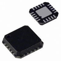
ADP5020ACPZ-R7 Analog Devices Inc, ADP5020ACPZ-R7 Datasheet - Page 4

ADP5020ACPZ-R7
Manufacturer Part Number
ADP5020ACPZ-R7
Description
IC REG LDO DUAL BUCK 20LFCSP
Manufacturer
Analog Devices Inc
Datasheet
1.ADP5020ACPZ-R7.pdf
(28 pages)
Specifications of ADP5020ACPZ-R7
Design Resources
Powering AD9272 with ADP5020 Switching Regulator PMU for Increased Efficiency (CN0135)
Applications
Handheld/Mobile Devices
Current - Supply
10mA
Voltage - Supply
2.4 V ~ 5.5 V
Operating Temperature
-40°C ~ 85°C
Mounting Type
Surface Mount
Package / Case
20-LFCSP
Supply Voltage
5.5V
No. Of Step-down Dc - Dc Converters
2
No. Of Ldo Regulators
1
Digital Ic Case Style
LFCSP
No. Of Pins
20
No. Of Regulated Outputs
3
Operating Temperature Range
-40°C To
Lead Free Status / RoHS Status
Lead free / RoHS Compliant
Other names
ADP5020ACPZ-R7TR
ADP5020
SPECIFICATIONS
T
Table 1.
Parameter
OPERATING RANGE
EN, SDA, SCL CHARACTERISTICS
INPUT LOGIC CURRENT
XSHTDN, EN/GPIO
OUTPUT LOGIC LEAKAGE CURRENT
UNDERVOLTAGE LOCKOUT THRESHOLD
POWER-ON RESET THRESHOLD
UVLO GLITCH DEBOUNCE TIME
SHUTDOWN OUTPUT DURATION
POWER GOOD (POK) ACTIVATION DELAY TIME
NO LOAD CURRENT CHARACTERISTICS
THERMAL CHARACTERISTICS
HOUSEKEEPING BLOCK
1
2
3
4
The V
Shutdown output duration is automatic when using the EN pin. To get this delay when using I
Activation delays apply only when the device is activated through the EN pin or the EN_ALL bit (Address 0x03[4]); the sequencer controls the turning on of the
regulators.
The quiescent current is calculated as though all regulators are powered up.
J
VDDx Operating Voltage Range
Logic I/O Operating Voltage Range
Low Level Input Voltage
High Level Input Voltage
Low Level Output Voltage
High Level Output Voltage
Falling
Rising
Falling
Rising
EN to First Regulator
First to Second Regulator
Second to Third Regulator
Standby Current
Lockout Current
Operating Quiescent Current, Switching
Thermal Shutdown, T
Thermal Shutdown Hysteresis
Power Good Threshold
= −40°C to +125°C, V
DD_IO
voltage must be less than or equal to the level on the V
J
Rising
DDx
= 3.6 V, V
2
1
DD_IO
4
= 1.8 V, unless otherwise noted.
3
Symbol
V
V
V
V
I
V
V
I
V
V
V
V
t
t
t
t
I
I
I
T
V
LK
LK
Q(STNBY)
LOCK
Q
XSHTDN
REG1
REG2
REG3
DDx
SD
DD
DD_IO
IL
IH
OL
OH
UVLOF
UVLOR
PORF
PORR
PG
supply lines.
Rev. 0 | Page 4 of 28
Conditions
Internal pull-down, 1 MΩ
I
I
Referenced to V
Referenced to V
Referenced to V
Referenced to V
V
XSHTDN line driven low
EN = 0
EN = 0, V
I
RST
RST
LOAD
DD
= +3 mA
= −3 mA
> POR levels
= 0 mA
DDA
< V
2
C, FORCE_XS must be set to 1.
UVLOF
DDA
DDA
DDA
DDA
Min
2.4
1.7
0.7 × V
−1
0.8 × V
1.8
1.0
70
DD_IO
DD_IO
Typ
2.0
2.2
1.4
1.6
50
1
5
5
5
1
1
10
150
30
80
Max
5.5
3.6
0.3 × V
+6
0.2 × V
1
2.4
1.7
5
1
15
90
DD_IO
DD_IO
Unit
V
V
V
V
μA
V
V
μA
V
V
V
V
μs
ms
ms
ms
ms
μA
μA
mA
°C
°C
%


