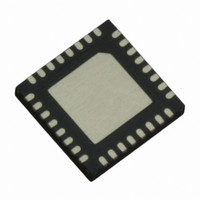
IR3503MTRPBF International Rectifier, IR3503MTRPBF Datasheet - Page 10

IR3503MTRPBF
Manufacturer Part Number
IR3503MTRPBF
Description
IC CTRL XPHASE VR11.0/1 32-MLPQ
Manufacturer
International Rectifier
Series
XPhase3™r
Datasheet
1.IR3503MTRPBF.pdf
(39 pages)
Specifications of IR3503MTRPBF
Applications
Processor
Current - Supply
8mA
Voltage - Supply
4.75 V ~ 7.5 V
Operating Temperature
0°C ~ 100°C
Mounting Type
Surface Mount
Package / Case
*
Package
32-Lead MLPQ
Circuit
X-Phase Control IC
Switch Freq (khz)
250kHz to 1.5MHz
Pbf
PbF Option Available
Lead Free Status / RoHS Status
Lead free / RoHS Compliant
Other names
IR3503MTRPBFTR
APPLICATION SYSTEM CIRCUIT
PWM Control Method
The system block diagram of the XPhase3
trailing edge modulation is used. A high-gain wide-bandwidth voltage type error amplifier in the control IC is used for
the voltage control loop. Input voltage is sensed in phase ICs and feed-forward control is realized. The PWM ramp
slope will change with the input voltage and automatically compensate for changes in the input voltage. The input
voltage can change due to variations in the silver box output voltage or due to the wire and PCB-trace voltage drop
related to changes in load current.
Frequency and Phase Timing Control
The oscillator is located in the control IC and the system clock frequency is programmable from 250 kHz to 9 MHZ by
an external resistor. The control IC system clock signal CLKOUT is connected to CLKIN of all the phase ICs. The
phase timing of the phase ICs is controlled by the daisy chain loop, where control IC phase clock output PHSOUT is
connected to the phase clock input PHSIN of the first phase IC, and PHSOUT of the first phase IC is connected to
PHSIN of the second phase IC, etc. The PHSOUT of the last phase IC is connected back to PHSIN of the control IC.
ENABLE
VRRDY
VRHOT
PSI#
IOUT
VID7
VID6
VID5
VID4
VID3
VID2
VID1
VID0
CMON
VOSEN-
RMON
4.75V to 7.5V VCCL
Page 10 of 39
RMON1
+12V
RHOTSET2
CVCCL
33
1
2
3
4
5
6
7
8
EXPAD
VID7
VID6
VID5
VID4
VID3
VID2
VID1
VID0
RHOTSET1
Note: Pin 33 of IR3503 is the exposed pad located under the IC. It is connected to IC ground
IR3503
VDAC_BUFF
RFB
VSETPT
SS/DEL
ROSC
VDAC
VDRP
PSI#
RFB1
VN
24
23
22
21
20
19
18
17
CFB
ROSC
RDRP
RVDAC
RSETPT
RTCMP2
RCP
RTCMP1
RTCMP3
CCP1
VOSEN+
VOSEN-
Figure 4: IR3503 Multiphase Application Circuit
CSS/DEL
CCP
TM
CVDAC
RTHERM
architecture is shown in Figure 3. Feed-forward voltage mode control with
1
2
3
4
5
1
2
3
4
5
1
2
3
4
5
1
2
3
4
5
ILL
PSI#
DACIN
LGND
PHSIN
ILL
PSI#
DACIN
LGND
PHSIN
ILL
PSI#
DACIN
LGND
PHSIN
ILL
PSI#
DACIN
LGND
PHSIN
IR3529
IR3529
IR3529
IR3529
GATEH
BOOST
OCSET
GATEH
BOOST
OCSET
GATEH
BOOST
OCSET
GATEH
BOOST
OCSET
VCCL
VCCL
VCCL
VCCL
SW
SW
SW
SW
15
14
13
12
11
15
14
13
12
11
15
14
13
12
11
15
14
13
12
11
CBST1
CVCCL2
CBST2
CVCCL3
CBST3
CVCCL4
CBST4
CVCCL5
ROCP1
COCP1
ROCP2
COCP2
ROCP3
COCP3
ROCP4
COCP4
February 12, 2010
IR3503
RCS1
RCS2
RCS3
RCS4
L1
L2
L3
L4
COUT1
CCS1
CCS2
CCS3
CCS4
VOUT+
VOUT-
VOSEN+
VOSEN-


