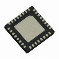
IR3503MTRPBF International Rectifier, IR3503MTRPBF Datasheet - Page 15

IR3503MTRPBF
Manufacturer Part Number
IR3503MTRPBF
Description
IC CTRL XPHASE VR11.0/1 32-MLPQ
Manufacturer
International Rectifier
Series
XPhase3™r
Datasheet
1.IR3503MTRPBF.pdf
(39 pages)
Specifications of IR3503MTRPBF
Applications
Processor
Current - Supply
8mA
Voltage - Supply
4.75 V ~ 7.5 V
Operating Temperature
0°C ~ 100°C
Mounting Type
Surface Mount
Package / Case
*
Package
32-Lead MLPQ
Circuit
X-Phase Control IC
Switch Freq (khz)
250kHz to 1.5MHz
Pbf
PbF Option Available
Lead Free Status / RoHS Status
Lead free / RoHS Compliant
Other names
IR3503MTRPBFTR
Adaptive Voltage Positioning (AVP)
Adaptive voltage positioning is needed to optimize the output voltage excursions during dynamic load variations. The
objective of AVP is to control the output voltage to a value that is slightly higher than the minimum value at full load and
slightly lower than the maximum permissible limit at light load. Thus, AVP also helps to reduce the output power at full
load and is essential to meet the load line specifications. The circuitry related to voltage positioning is shown in Figure
9. The output voltage is set by the reference voltage VSETPT at the positive input to the error amplifier. This reference
voltage can be programmed to have a constant DC offset below the VDAC by connecting RSETPT between VDAC
and VSETPT. The IVSETPT is controlled by the resistor, ROSC.
The average load current information for all the phases is fed back to the control IC through the IIN pin. As shown in
Figure 9, this information is thermally compensated with some gain by a set of buffer and thermal compensation
amplifiers to generate the voltage at the VDRP pin. The VDRP pin is connected to the FB pin through the resistor
R
additional current will flow into the FB pin equal to (VDRP-VDAC) / R
voltage increases accordingly. More current flows through the feedback resistor R
more droop. The resistor R
The positioning voltage can be programmed by the resistor R
converter output impedance. The offset and slope of the converter output impedance are referenced to and therefore
independent of the VDAC voltage.
DRP
. Since the error amplifier will force the loop to maintain FB to be equal to the VDAC reference voltage, an
Page 15 of 39
VDAC1
+
-
VDAC
Buffer
Control IC
Figure 9: Adaptive Voltage Positioning (AVP) with Thermal Compensation
Remote
Sense
Amplifier
Thermal
Comp
Amplifier
Rinternal2
DRP
produces the required droop in output voltage proportional to the load current.
VSETPT
+
-
+
-
Error
Amplifier
Rinternal1
+
-
∆
i
V
=
DRP
V
DRP
=
EAOUT
R
FB
IIN
VDAC
VDRP
DAC_BUFF
VN
VO
VOSEN+
VOSEN-
i
DRP
−
*
V
R
DAC
FB
RTCMP2
RDRP
=
RTCMP3
RTCMP1
I
RFB
OUT
DRP
RTHERM1
×
so that the droop impedance produces the desired
R
DRP
loadline
. When the load current increases, the VDRP
VDAC
VDAC
IOUT
IOUT
FB
Phase IC
Phase IC
3k
3k
February 12, 2010
and causes the output to have
IR3503
Current
Sense
Amplifier
Current
Sense
Amplifier
+
+
-
-
CSIN+
CSIN+
CSIN-
CSIN-


