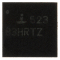
ISL62383HRTZ Intersil, ISL62383HRTZ Datasheet - Page 8

ISL62383HRTZ
Manufacturer Part Number
ISL62383HRTZ
Description
IC PWR SUPPLY CONTROLLER 28TQFN
Manufacturer
Intersil
Datasheet
1.ISL62383HRTZ.pdf
(23 pages)
Specifications of ISL62383HRTZ
Applications
Power Supply Controller
Voltage - Supply
5.5 V ~ 25 V
Current - Supply
150µA
Operating Temperature
-10°C ~ 100°C
Mounting Type
Surface Mount
Package / Case
28-TQFN
Rohs Compliant
YES
Lead Free Status / RoHS Status
Lead free / RoHS Compliant
Voltage - Input
-
Available stocks
Company
Part Number
Manufacturer
Quantity
Price
Company:
Part Number:
ISL62383HRTZ
Manufacturer:
AD
Quantity:
655
Pin Descriptions
28 LD
PIN NUMBER
10
12
13
14
15
16
17
18
19
20
21
22
23
24
25
26
27
11
1
2
3
4
5
6
7
8
9
-
-
-
-
32 LD
10
11
12
13
14
15
16
17
18
19
20
21
22
23
24
25
26
27
28
29
30
31
1
2
3
4
5
6
7
8
9
PGOOD2 SMPS2 open-drain power-good status output. Connect to LDO5 through a 100k resistor. Output will be high when
PGOOD1 SMPS1 open-drain power-good status output. Connect to LDO5 through a 100k resistor. Output will be high when
LDO3EN Logic input for enabling and disabling the LDO3 linear regulator. Positive logic input.
OCSET1 Input from current-sensing network used to program the overcurrent shutdown threshold for SMPS1.
OCSET2 Input from current-sensing network used to program the over-current shutdown threshold for SMPS2.
PHASE1 SMPS1 switching node for high-side gate drive return and synthetic ripple modulation. Connect to the switching
UGATE1 High-side NMOS gate drive output for SMPS1. Connect to the gate of the SMPS1 switching FET.
LDO3FB LDO3 linear regulator feedback input used for output voltage programming and regulation.
UGATE2 High-side NMOS gate drive output for SMPS2. Connect to the gate of the SMPS2 switching FET.
PHASE2 SMPS2 switching node for high-side gate drive return and synthetic ripple modulation. Connect to the switching
LGATE1
LGATE2
LDO3IN
BOOT1
BOOT2
VOUT1
VOUT2
FSET2
FSET1
NAME
FCCM
ISEN1
PGND
ISEN2
VCC2
VCC1
LDO3
LDO5
EN1
EN2
FB1
VIN
the SMPS2 output is within the regulation window with no faults detected.
Frequency control input for SMPS2. Connect a resistor to ground to program the switching frequency. A small
ceramic capacitor such as 10nF is necessary to parallel with this resistor to smooth the voltage.
Logic input to control efficiency mode. Logic high forces continuous conduction mode (CCM). Logic low allows full
discontinuous conduction mode (DCM). Float this pin for ultrasonic DCM operation.
SMPS2 analog power supply input for reference voltages and currents. Connect to VCC1 with a 10Ω resistor.
Bypass to ground with a 1µF ceramic capacitor near the IC.
SMPS1 analog power supply input for reference voltages and currents. It is internally connected to the LDO5
output. Bypass to ground with a 1µF ceramic capacitor near the IC.
Frequency control input for SMPS1. Connect a resistor to ground to program the switching frequency. A small
ceramic capacitor such as 10nF is necessary to parallel with this resistor to smooth the voltage.
the SMPS1 output is within the regulation window with no faults detected.
SMPS1 feedback input used for output voltage programming and regulation.
SMPS1 output voltage sense input. Used for soft-discharge.
SMPS1 current sense input. Used for ove-current protection and R
Logic input to enable and disable SMPS1. A logic high will enable SMPS1 immediately. A logic low will disable
SMPS1. Floating this input will delay SMPS1 start-up until after SMPS2 achieves regulation.
NMOS source, the synchronous NMOS drain, and the output inductor for SMPS1.
SMPS1 bootstrap input for the switching NMOS gate drivers. Connect to PHASE1 with a 0.22µF ceramic capacitor.
Low-side NMOS gate drive output for SMPS1. Connect to the gate of the SMPS1 synchronous FET.
LDO3 linear regulator output, providing up to 100mA. Bypass to ground with a 4.7µF ceramic capacitor.
Power input for LDO3. Must be connected to a voltage greater than the LDO3 set point plus the dropout voltage.
Feed-forward input for line voltage transient compensation. Connect to the power train input voltage.
5V linear regulator output, providing up to 100mA before switchover to SMPS2. Bypass to ground with a 4.7µF
ceramic capacitor.
Power ground for SMPS1 and SMPS2. This provides a return path for synchronous FET switching currents.
Low-side NMOS gate drive output for SMPS2. Connect to the gate of the SMPS2 synchronous FET.
SMPS2 bootstrap input for the switching NMOS gate drivers. Connect to PHASE2 with a 0.22µF ceramic capacitor.
NMOS source, the synchronous NMOS drain, and the output inductor for SMPS2.
Logic input to enable and disable SMPS2. A logic high will enable SMPS2 immediately. A logic low will disable
SMPS2. Floating this input will delay SMPS2 start-up until after SMPS1 achieves regulation.
SMPS2 current sense input. Used for overcurrent protection and R
SMPS2 output voltage sense input. Used for soft-discharge and switchover to LDO5 output.
8
ISL62381, ISL62382, ISL62383
FUNCTION
3
3
regulation.
regulation.
August 7, 2008
FN6665.4


