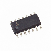
ISL6522BIBZ Intersil, ISL6522BIBZ Datasheet - Page 11

ISL6522BIBZ
Manufacturer Part Number
ISL6522BIBZ
Description
IC PWM BUCK BST VM 14SOIC
Manufacturer
Intersil
Datasheet
1.ISL6522BCBZ.pdf
(15 pages)
Specifications of ISL6522BIBZ
Pwm Type
Voltage Mode
Number Of Outputs
1
Frequency - Max
1MHz
Duty Cycle
100%
Voltage - Supply
10.8 V ~ 13.2 V
Buck
Yes
Boost
Yes
Flyback
No
Inverting
No
Doubler
No
Divider
No
Cuk
No
Isolated
No
Operating Temperature
-40°C ~ 85°C
Package / Case
14-SOIC (3.9mm Width), 14-SOL
Frequency-max
1MHz
Lead Free Status / RoHS Status
Lead free / RoHS Compliant
Available stocks
Company
Part Number
Manufacturer
Quantity
Price
Company:
Part Number:
ISL6522BIBZ-T
Manufacturer:
INTERSIL
Quantity:
9 100
The response time to a transient is different for the
application of load and the removal of load. The following
equations give the approximate response time interval for
application and removal of a transient load:
where: I
response time to the application of load, and t
response time to the removal of load. With a +5V input
source, the worst case response time can be either at the
application or removal of load and dependent upon the
output voltage setting. Be sure to check both of these
equations at the minimum and maximum output levels for
the worst case response time.
Input Capacitor Selection
Use a mix of input bypass capacitors to control the voltage
overshoot across the MOSFETs. Use small ceramic
capacitors for high frequency decoupling and bulk capacitors
to supply the current needed each time Q1 turns on. Place
the small ceramic capacitors physically close to the
MOSFETs and between the drain of Q1 and the source of Q2.
The important parameters for the bulk input capacitor are the
voltage rating and the RMS current rating. For reliable
operation, select the bulk capacitor with voltage and current
ratings above the maximum input voltage and largest RMS
current required by the circuit. The capacitor voltage rating
should be at least 1.25 times greater than the maximum
input voltage and a voltage rating of 1.5 times is a
conservative guideline. The RMS current rating requirement
for the input capacitor of a buck regulator is approximately
1/2 the DC load current.
For a through-hole design, several electrolytic capacitors
(Panasonic HFQ series or Nichicon PL series or Sanyo
MV-GX or equivalent) may be needed. For surface mount
designs, solid tantalum capacitors can be used, but caution
must be exercised with regard to the capacitor surge current
rating. These capacitors must be capable of handling the
surge-current at power-up. The TPS series available from
AVX, and the 593D series from Sprague are both surge
current tested.
MOSFET Selection/Considerations
The ISL6522B requires two N-Channel power MOSFETs.
These should be selected based upon r
requirements, and thermal management requirements.
In high-current applications, the MOSFET power dissipation,
package selection and heatsink are the dominant design
factors. The power dissipation includes two loss
components; conduction loss and switching loss. The
conduction losses are the largest component of power
dissipation for both the upper and the lower MOSFETs.
These losses are distributed between the two MOSFETs
t
RISE
=
TRAN
------------------------------- -
V
L
O
IN
×
–
I
V
TRAN
is the transient load current step, t
OUT
t
FALL
11
=
L
------------------------------ -
O
V
×
OUT
I
TRAN
DS(ON)
FALL
, gate supply
RISE
is the
is the
ISL6522B
according to duty factor. The switching losses seen when
sourcing current will be different from the switching losses seen
when sinking current. When sourcing current, the upper
MOSFET realizes most of the switching losses. The lower
switch realizes most of the switching losses when the converter
is sinking current (see the equations below).
These equations assume linear voltage-current transitions
and do not adequately model power loss due the reverse-
recovery of the upper and lower MOSFET’s body diode. The
gate-charge losses are dissipated by the ISL6522B and do
not heat the MOSFETs. However, large gate-charge
increases the switching interval, t
upper MOSFET switching losses. Ensure that both
MOSFETs are within their maximum junction temperature at
high ambient temperature by calculating the temperature
rise according to package thermal-resistance specifications.
A separate heatsink may be necessary depending upon
MOSFET power, package type, ambient temperature and air
flow.
Standard-gate MOSFETs are normally recommended for
use with the ISL6522B. However, logic-level gate MOSFETs
can be used under special circumstances. The input voltage,
upper gate drive level, and the MOSFETs absolute gate-to-
source voltage rating determine whether logic-level
MOSFETs are appropriate.
Figure 9 shows the upper gate drive (BOOT pin) supplied by
a bootstrap circuit from V
develops a floating supply voltage referenced to the PHASE
pin. This supply is refreshed each cycle to a voltage of V
less the boot diode drop (V
turns on. A logic-level MOSFET can only be used for Q1 if
the MOSFETs absolute gate-to-source voltage rating
exceeds the maximum voltage applied to V
logic-level MOSFET can be used if its absolute gate-to-
source voltage rating exceeds the maximum voltage applied
to PVCC.
Losses while Sinking Current
Losses while Sourcing Current
P
P
P
P
UPPER
LOWER
LOWER
UPPER
Where: D is the duty cycle = V
= Io
= Io
=
=
t
F
SW
Io
S
Io
2
2
2
is the switching frequency.
2
x r
x r
is the switching interval, and
×
×
DS(ON)
r
DS(ON)
r
DS ON
DS ON
(
(
x D
x (1 - D)
)
CC
)
×
×
D
D
(
. The boot capacitor, C
) when the lower MOSFET, Q2
1 D
+
–
1
-- - Io
2
OUT
⋅
SW
)
+
×
/ V
1
-- - Io
2
which increases the
V
⋅
IN
IN
,
×
×
CC
V
t
SW
IN
. For Q2, a
×
×
t
F
SW
S
BOOT
×
F
S
CC


