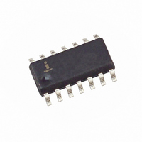
ISL6522BIBZ Intersil, ISL6522BIBZ Datasheet - Page 8

ISL6522BIBZ
Manufacturer Part Number
ISL6522BIBZ
Description
IC PWM BUCK BST VM 14SOIC
Manufacturer
Intersil
Datasheet
1.ISL6522BCBZ.pdf
(15 pages)
Specifications of ISL6522BIBZ
Pwm Type
Voltage Mode
Number Of Outputs
1
Frequency - Max
1MHz
Duty Cycle
100%
Voltage - Supply
10.8 V ~ 13.2 V
Buck
Yes
Boost
Yes
Flyback
No
Inverting
No
Doubler
No
Divider
No
Cuk
No
Isolated
No
Operating Temperature
-40°C ~ 85°C
Package / Case
14-SOIC (3.9mm Width), 14-SOL
Frequency-max
1MHz
Lead Free Status / RoHS Status
Lead free / RoHS Compliant
Available stocks
Company
Part Number
Manufacturer
Quantity
Price
Company:
Part Number:
ISL6522BIBZ-T
Manufacturer:
INTERSIL
Quantity:
9 100
Overcurrent Protection
The overcurrent function protects the converter from a
shorted output by using the upper MOSFETs on-resistance,
r
converter’s efficiency and reduces cost by eliminating a
current sensing resistor.
The overcurrent function cycles the soft-start function in a
hiccup mode to provide fault protection. A resistor (R
programs the overcurrent trip level. An internal 200µA
(typical) current sink develops a voltage across R
is in reference to V
MOSFET (also referenced to V
across R
sequence. The soft-start function discharges C
10µA current sink and inhibits PWM operation. The soft-start
function recharges C
the error amplifier clamped to the SS voltage. Should an
overload occur while recharging C
inhibits PWM operation while fully charging C
complete its cycle. Figure 4 shows this operation with an
overload condition. Note that the inductor current increases
to over 15A during the C
overcurrent trip. The converter dissipates very little power
with this method. The measured input power for the
conditions of Figure 4 is 2.5W.
The overcurrent function will trip at a peak inductor current
(I
where I
is typical). The OC trip point varies mainly due to the
MOSFETs r
in the normal operating load range, find the R
from the equation above with:
The maximum r
For an equation for the ripple current see the section under
component guidelines titled Output Inductor Selection.
A small ceramic capacitor should be placed in parallel with
R
presence of switching noise on the input voltage.
Current Sinking
The ISL6522B incorporates a MOSFET shoot-through
protection method which allows a converter to sink current
as well as source current. Care should be exercised when
designing a converter with the ISL6522B when it is known
that the converter may sink current.
I
DS(ON)
1. The minimum I
2. Determine
PEAK
PEAK)
OCSET
where ∆I is the output inductor ripple current.
=
OCSET
determined by:
to monitor the current. This method enhances the
OCSET
to smooth the voltage across R
I
-------------------------------------------------- -
OCSET
DS(ON)
r
DS ON
is the internal OCSET current source (200µA
I
, the overcurrent function initiates a soft-start
DS(ON)
PEAK
•
(
R
IN
OCSET
variations. To avoid overcurrent tripping
OCSET
. When the voltage across the upper
SS
)
for I
at the highest junction temperature.
, and PWM operation resumes with
SS
PEAK
from the specification table.
charging interval and causes an
8
>
IN
I
) exceeds the voltage
OUT MAX
SS
, the soft-start function
(
OCSET
)
+
OCSET
(
SS
∆I
SS
) 2 ⁄
in the
OCSET
to 4V to
with a
,
OCSET
resistor
that
ISL6522B
)
When the converter is sinking current, it is behaving as a
boost converter that is regulating its input voltage. This
means that the converter is boosting current into the V
the voltage that is being down-converted. If there is nowhere
for this current to go, such as to other distributed loads on
the V
other methods, the capacitance on the V
the current. This situation will cause the voltage level of the
V
to a level that exceeds the maximum voltage rating of the
MOSFETs or the input capacitors, damage may occur to
these parts. If the bias voltage for the ISL6522B comes from
the V
ISL6522B may be exceeded and the IC will experience a
catastrophic failure and the converter will no longer be
operational. Ensuring that there is a path for the current to
follow other than the capacitance on the rail will prevent
these failure modes.
Application Guidelines
Layout Considerations
As in any high frequency switching converter, layout is very
important. Switching current from one power device to
another can generate voltage transients across the
impedances of the interconnecting bond wires and circuit
traces. These interconnecting impedances should be
minimized by using wide, short printed circuit traces. The
critical components should be located as close together as
possible using ground plane construction or single point
grounding.
Figure 5 shows the critical power components of the
converter. To minimize the voltage overshoot the
interconnecting wires indicated by heavy lines should be part
of ground or power plane in a printed circuit board. The
components shown in Figure 6 should be located as close
together as possible. Please note that the capacitors C
and C
Locate the ISL6522B within three inches of the MOSFETs,
Q1 and Q2. The circuit traces for the MOSFETs’ gate and
source connections from the ISL6522B must be sized to
handle up to 1A peak current.
IN
FIGURE 5. PRINTED CIRCUIT BOARD POWER AND
ISL6522B
rail to increase. If the voltage level of the rail is boosted
IN
IN
O
rail, through a voltage limiting protection device, or
rail, then the maximum voltage rating of the
each represent numerous physical capacitors.
UGATE
PHASE
LGATE
PGND
GROUND PLANES OR ISLANDS
V
Q2
Q1
RETURN
IN
D2
C
IN
IN
L
bus will absorb
O
C
O
V
OUT
IN
IN
rail,


