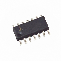
ISL6522BIBZ Intersil, ISL6522BIBZ Datasheet - Page 9

ISL6522BIBZ
Manufacturer Part Number
ISL6522BIBZ
Description
IC PWM BUCK BST VM 14SOIC
Manufacturer
Intersil
Datasheet
1.ISL6522BCBZ.pdf
(15 pages)
Specifications of ISL6522BIBZ
Pwm Type
Voltage Mode
Number Of Outputs
1
Frequency - Max
1MHz
Duty Cycle
100%
Voltage - Supply
10.8 V ~ 13.2 V
Buck
Yes
Boost
Yes
Flyback
No
Inverting
No
Doubler
No
Divider
No
Cuk
No
Isolated
No
Operating Temperature
-40°C ~ 85°C
Package / Case
14-SOIC (3.9mm Width), 14-SOL
Frequency-max
1MHz
Lead Free Status / RoHS Status
Lead free / RoHS Compliant
Available stocks
Company
Part Number
Manufacturer
Quantity
Price
Company:
Part Number:
ISL6522BIBZ-T
Manufacturer:
INTERSIL
Quantity:
9 100
Figure 6 shows the circuit traces that require additional
layout consideration. Use single point and ground plane
construction for the circuits shown. Minimize any leakage
current paths on the SS PIN and locate the capacitor, C
close to the SS pin because the internal current source is
only 10µA. Provide local V
GND pins. Locate the capacitor, C
to the BOOT and PHASE pins.
Feedback Compensation
Figure 7 highlights the voltage-mode control loop for a
synchronous rectified buck converter. The output voltage
(V
amplifier (error amp) output (V
oscillator (OSC) triangular wave to provide a pulse-width
modulated (PWM) wave with an amplitude of V
PHASE node. The PWM wave is smoothed by the output filter
(L
The modulator transfer function is the small-signal transfer
function of V
gain and the output filter (L
break frequency at F
the modulator is simply the input voltage (V
peak-to-peak oscillator voltage ∆V
O
OUT
C
FIGURE 6. PRINTED CIRCUIT BOARD SMALL SIGNAL
SS
SS
and C
) is regulated to the reference voltage level. The error
ISL6522B
O
GND
).
OUT
LAYOUT GUIDELINES
/V
E/A
LC
C
PHASE
VCC
BOOT
. This function is dominated by a DC
BOOT
and a zero at F
+12V
CC
O
and C
C
decoupling between VCC and
9
E/A
VCC
D1
BOOT
) is compared with the
OSC
O
), with a double pole
.
ESR
as close as practical
Q1
+V
Q2
IN
IN
. The DC gain of
L
) divided by the
O
IN
C
O
at the
V
SS
OUT
ISL6522B
Modulator Break Frequency Equations
The compensation network consists of the error amplifier
(internal to the ISL6522B) and the impedance networks Z
and Z
a closed loop transfer function with the highest 0dB crossing
frequency (f
is the difference between the closed loop phase at f
180 degrees. The equations below relate the compensation
network’s poles, zeros and gain to the components (R1, R2,
R3, C1, C2, and C3) in Figure 8. Use these guidelines for
locating the poles and zeros of the compensation network:
Compensation Break Frequency Equations
F
F
F
1. Pick Gain (R2/R1) for desired converter bandwidth
2. Place 1
LC
Z1
Z2
∆V
FIGURE 7. VOLTAGE - MODE BUCK CONVERTER
(~75% F
=
OSC
=
=
FB
-------------------------------------- -
2π
----------------------------------
2π R
----------------------------------------------------- -
2π
. The goal of the compensation network is to provide
OSC
•
•
•
(
ST
0dB
L
R1
COMPARATOR
1
1
LC
2 C1
O
COMPENSATION DESIGN
ERROR
AMP
V
•
Zero Below Filter’s Double Pole
ISL6522B
•
)
) and adequate phase margin. Phase margin
+
1
E/A
DETAILED COMPENSATION COMPONENTS
PWM
C
R3
O
Z
+
-
COMP
FB
+
) C3
-
C1
•
REFERENCE
C2
+
-
R2
F
DRIVER
DRIVER
REF
ESR
Z
IN
F
F
P1
P2
=
Z
FB
FB
=
=
-------------------------------------------- -
2π
V
----------------------------------
2π R3 C3
------------------------------------------------------ -
2π R2
IN
•
PHASE
•
(
C3
•
(PARASITIC)
ESR C
1
Z
1
L
IN
R1
O
•
•
•
R3
1
ESR
--------------------- -
C1
C1 C2
C
V
O
O
OUT
)
+
•
0dB
C2
V
OUT
and
IN


