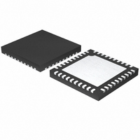
ISL6326CRZ-T Intersil, ISL6326CRZ-T Datasheet - Page 25

ISL6326CRZ-T
Manufacturer Part Number
ISL6326CRZ-T
Description
IC CTRLR PWM 4PHASE BUCK 40-QFN
Manufacturer
Intersil
Datasheet
1.ISL6326CRZ.pdf
(30 pages)
Specifications of ISL6326CRZ-T
Pwm Type
Voltage Mode
Number Of Outputs
1
Frequency - Max
275kHz
Duty Cycle
25%
Voltage - Supply
4.75 V ~ 5.25 V
Buck
Yes
Boost
No
Flyback
No
Inverting
No
Doubler
No
Divider
No
Cuk
No
Isolated
No
Operating Temperature
0°C ~ 70°C
Package / Case
40-VFQFN, 40-VFQFPN
Frequency-max
275kHz
Lead Free Status / RoHS Status
Lead free / RoHS Compliant
Available stocks
Company
Part Number
Manufacturer
Quantity
Price
Part Number:
ISL6326CRZ-T
Manufacturer:
INTERSIL
Quantity:
20 000
conducted through the upper MOSFET across VIN. The
power dissipated as a result is P
Finally, the resistive part of the upper MOSFET’s is given in
Equation 29 as P
The total power dissipated by the upper MOSFET at full load
can now be approximated as the summation of the results
from Equations 26, 27, and 28. Since the power equations
depend on MOSFET parameters, choosing the correct
MOSFETs can be an iterative process involving repetitive
solutions to the loss equations for different MOSFETs and
different switching frequencies.
Current Sensing Resistor
The resistors connected to the ISEN+ pins determine the
gains in the load-line regulation loop and the channel-current
balance loop as well as setting the overcurrent trip point.
Select values for these resistors by using Equation 30:
where R
ISEN+ pin, N is the active channel number, R
resistance of the current sense element, either the DCR of
the inductor or R
and I
can be chosen to be 1.3x the maximum load current of the
specific application.
With integrated temperature compensation, the sensed
current signal is independent on the operational temperature
of the power stage, i.e. the temperature effect on the current
sense element R
temperature compensation function. R
should be the resistance of the current sense element at the
room temperature.
When the integrated temperature compensation function is
disabled by pulling the TCOMP pin to GND, the sensed
current will be dependent on the operational temperature of
the power stage, since the DC resistance of the current
sense element may be changed according to the operational
temperature. R
resistance of the current sense element at the all-operational
temperature.
In certain circumstances, it may be necessary to adjust the
value of one or more ISEN resistors. When the components
of one or more channels are inhibited from effectively
dissipating their heat so that the affected channels run hotter
than desired, choose new, smaller values of RISEN for the
affected phases (see the section entitled “Channel-Current
P
P
R
UP 4 ,
UP 3 ,
ISEN
OCP
≈
=
=
r
DS ON
ISEN
V
---------------------- -
85 10
is the desired overcurrent trip point. Typically, I
IN
(
R
×
Q
X
is the sense resistor connected to the
rr
)
X
–
f
S
⎛
⎜
⎝
6
SENSE
X
in Equation 30 should be the maximum DC
UP,4
I
----- -
N
M
I
------------- -
OCP
is cancelled by the integrated
⎞
⎟
⎠
N
2
.
d
+
depending on the sensing method,
I
--------- - d
PP
12
2
25
UP,3
and is approximately
X
in Equation 30
X
is the
(EQ. 29)
(EQ. 28)
(EQ. 30)
OCP
ISL6326
Balance” on page 13). Choose R
desired decrease in temperature rise in order to cause
proportionally less current to flow in the hotter phase in
Equation 31:
Make sure that ΔT
ambient temperature, and ΔT
rise above the ambient temperature. While a single
adjustment according to Equation 31 is usually sufficient, it
may occasionally be necessary to adjust R
times to achieve optimal thermal balance between all
channels.
Load-Line Regulation Resistor
The load-line regulation resistor is labelled R
Its value depends on the desired loadline requirement of the
application.
The desired loadline can be calculated by using
Equation 32:
where I
and VR
load condition.
Based on the desired loadline R
resistor can be calculated by using Equation 33:
where N is the active channel number, R
resistor connected to the ISEN+ pin, and R
resistance of the current sense element, either the DCR of
the inductor or R
If one or more of the current sense resistors are adjusted for
thermal balance, as in Equation 31, the load-line regulation
resistor should be selected based on the average value of
the current sensing resistors, as given in Equation 34:
where R
the n
Compensation
The two opposing goals of compensating the voltage
regulator are stability and speed. Depending on whether the
regulator employs the optional load-line regulation as
described in “Load-Line Regulation” on page 18, there are
two distinct methods for achieving these goals.
R
R
R
R
ISEN 2 ,
LL
FB
FB
=
th
=
=
V
------------------------ -
ISEN+ pin.
FL
N R
--------------------------------- -
R
----------
DROOP
R
DROOP
ISEN(n)
=
LL
X
I
is the full load current of the specific application,
FL
ISEN
R
R
∑
ISEN
n
X
R
R
is the desired voltage droop under the full
ISEN n ( )
is the current sensing resistor connected to
SENSE
LL
ΔT
----------
ΔT
2
is the desired temperature rise above the
2
1
depending on the sensing method.
1
is the measured temperature
LL
ISEN,2
, the loadline regulation
in proportion to the
ISEN
ISEN
X
FB
is the
is the sense
two or more
in Figure 5.
May 5, 2008
(EQ. 33)
(EQ. 34)
(EQ. 31)
(EQ. 32)
FN9262.1


