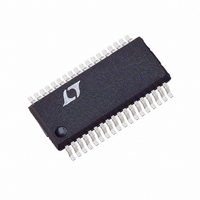
LTC3719EG Linear Technology, LTC3719EG Datasheet - Page 17

LTC3719EG
Manufacturer Part Number
LTC3719EG
Description
IC SW REG SYNC STEP-DOWN 36-SSOP
Manufacturer
Linear Technology
Datasheet
1.LTC3719EG.pdf
(32 pages)
Specifications of LTC3719EG
Applications
Controller, AMD Opteron™
Voltage - Input
4 ~ 36 V
Number Of Outputs
1
Voltage - Output
0.8 ~ 1.55 V
Operating Temperature
-40°C ~ 85°C
Mounting Type
Surface Mount
Package / Case
36-SSOP
Lead Free Status / RoHS Status
Contains lead / RoHS non-compliant
Available stocks
Company
Part Number
Manufacturer
Quantity
Price
Part Number:
LTC3719EG
Manufacturer:
LINEAR/凌特
Quantity:
20 000
Part Number:
LTC3719EG#PBF
Manufacturer:
LT/凌特
Quantity:
20 000
Company:
Part Number:
LTC3719EG#TR
Manufacturer:
LT
Quantity:
2 300
Part Number:
LTC3719EG#TRPBF
Manufacturer:
LINEAR/凌特
Quantity:
20 000
APPLICATIO S I FOR ATIO
INTV
An internal P-channel low dropout regulator produces 5V
at the INTV
regulator powers the drivers and internal circuitry of the
LTC3719. The INTV
peak and must be bypassed to power ground with a
minimum of 4.7 F tantalum or electrolytic capacitor. An
additional 1 F ceramic capacitor placed very close to the
IC is recommended due to the extremely high instanta-
neous currents required by the MOSFET gate drivers.
High input voltage applications in which large MOSFETs
are being driven at high frequencies may cause the maxi-
mum junction temperature rating for the LTC3719 to be
exceeded. The supply current is dominated by the gate
charge supply current, in addition to the current drawn
from the differential amplifier output. The gate charge is
dependent on operating frequency as discussed in the
Efficiency Considerations section. The supply current can
either be supplied by the internal 5V regulator or via the
EXTV
is less than 4.7V, all of the INTV
by the internal 5V linear regulator. Power dissipation for
the IC is higher in this case by (I
efficiency is lowered. The junction temperature can be
estimated by using the equations given in Note 1 of the
Electrical Characteristics. For example, the LTC3719 V
current is limited to less than 24mA from a 24V supply:
Use of the EXTV
The input supply current should be measured while the
controller is operating in continuous mode at maximum
V
prevent the maximum junction temperature from being
exceeded.
EXTV
The LTC3719 contains an internal P-channel MOSFET
switch connected between the EXTV
IN
T
T
J
J
and the power dissipation calculated in order to
CC
CC
CC
= 70 C + (24mA)(24V)(85 C/W) = 119 C
= 70 C + (24mA)(5V)(85 C/W) = 80.2 C
Regulator
pin. When the voltage applied to the EXTV
Connection
CC
pin from the V
CC
pin reduces the junction temperature to:
CC
U
pin regulator can supply up to 50mA
U
IN
CC
supply pin. The INTV
load current is supplied
IN
W
)(V
CC
IN
and INTV
– INTV
U
CC
CC
CC
) and
pins.
pin
CC
IN
When the voltage applied to EXTV
internal regulator is turned off and an internal switch
closes, connecting the EXTV
thereby supplying internal and MOSFET gate driving power
to the IC. The switch remains closed as long as the voltage
applied to EXTV
MOSFET driver and control power to be derived from a
separate 5V supply during normal operation (4.7V <
V
external 5V supply is not available. Do not apply greater
than 7V to the EXTV
0.3V when using the application circuits shown. If an
external voltage source is applied to the EXTV
the V
series with the LTC3719’s V
between the EXTV
from backfeeding V
Topside MOSFET Driver Supply (C
Functional Diagram)
External bootstrap capacitors C
the BOOST1 and BOOST2 pins supply the gate drive
voltages for the topside MOSFETs. Capacitor C
Functional Diagram is charged though diode D
INTV
turns on, the driver places the C
source of the desired MOSFET. This enhances the MOSFET
and turns on the topside switch. The switch node voltage,
SW, rises to V
The value of the boost capacitor C
times that of the total input capacitance of the topside
MOSFET(s). The reverse breakdown of D
than V
The final arbiter when defining the best gate drive ampli-
tude level will be the input supply current. If a change is
made that decreases input current, the efficiency has
improved. If the input current does not change then the
efficiency has not changed either.
EXTVCC
CC
IN
IN(MAX).
when the SW pin is low. When the topside MOSFET
supply is not present, a diode can be placed in
< 7V) and from the internal regulator when the
IN
and the BOOST pin rises to V
CC
CC
remains above 4.5V. This allows the
CC
IN
and the V
.
pin and ensure that EXTV
IN
CC
pin and a Schottky diode
IN
B
B1
voltage across the gate-
CC
pin to the INTV
B
pin, to prevent current
and C
needs to be 30 to 100
B
rises above 4.7V, the
,D
B
B
) (Refer to
B2
LTC3719
must be greater
connected to
IN
CC
+ V
CC
pin when
sn3719 3719fs
B
17
B
INTVCC
< V
CC
in the
from
IN
pin
+
.


