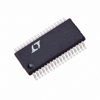
LTC3719EG Linear Technology, LTC3719EG Datasheet - Page 22

LTC3719EG
Manufacturer Part Number
LTC3719EG
Description
IC SW REG SYNC STEP-DOWN 36-SSOP
Manufacturer
Linear Technology
Datasheet
1.LTC3719EG.pdf
(32 pages)
Specifications of LTC3719EG
Applications
Controller, AMD Opteron™
Voltage - Input
4 ~ 36 V
Number Of Outputs
1
Voltage - Output
0.8 ~ 1.55 V
Operating Temperature
-40°C ~ 85°C
Mounting Type
Surface Mount
Package / Case
36-SSOP
Lead Free Status / RoHS Status
Contains lead / RoHS non-compliant
Available stocks
Company
Part Number
Manufacturer
Quantity
Price
Part Number:
LTC3719EG
Manufacturer:
LINEAR/凌特
Quantity:
20 000
Part Number:
LTC3719EG#PBF
Manufacturer:
LT/凌特
Quantity:
20 000
Company:
Part Number:
LTC3719EG#TR
Manufacturer:
LT
Quantity:
2 300
Part Number:
LTC3719EG#TRPBF
Manufacturer:
LINEAR/凌特
Quantity:
20 000
APPLICATIO S I FOR ATIO
LTC3719
22
Efficiency Considerations
The percent efficiency of a switching regulator is equal to
the output power divided by the input power times 100%.
It is often useful to analyze individual losses to determine
what is limiting the efficiency and which change would
produce the most improvement. Percent efficiency can be
expressed as:
where L1, L2, etc. are the individual losses as a percentage
of input power.
Although all dissipative elements in the circuit produce
losses, four main sources usually account for most of the
losses in LTC3719 circuits: 1) I
MOSFET transition losses, 3) INTV
and 4) LTC3719 V
differential amplifier output).
1) I
fuse (if used), MOSFET, inductor, current sense resistor,
and input and output capacitor ESR. In continuous mode
the average output current flows through L and R
but is “chopped” between the topside MOSFET and the
synchronous MOSFET. If the two MOSFETs have approxi-
mately the same R
MOSFET can simply be summed with the resistances of L,
R
R
total resistance is 25m . This results in losses ranging
from 2% to 8% as the output current increases from 3A to
15A per output stage for a 5V output, or a 3% to 12% loss
per output stage for a 3.3V output. Efficiency varies as the
inverse square of V
and output power level. The combined effects of increas-
ingly lower output voltages and higher currents required
by high performance digital systems is not doubling but
SENSE
DS(ON)
%Efficiency = 100% – (L1 + L2 + L3 + ...)
2
R losses are predicted from the DC resistances of the
and ESR to obtain I
= 10m , R
L
OUT
U
IN
= 10m , and R
DS(ON)
current (including loading on the
for the same external components
U
2
, then the resistance of one
R losses. For example, if each
2
R losses, 2) Topside
SENSE
W
CC
regulator current
= 5m , then the
U
SENSE
,
quadrupling the importance of loss terms in the switching
regulator system!
2) Transition losses apply only to the topside MOSFET(s),
and are significant only when operating at high input
voltages (typically 12V or greater). Transition losses can
be estimated from:
3) INTV
control currents. The MOSFET driver current results from
switching the gate capacitance of the power MOSFETs.
Each time a MOSFET gate is switched from low to high to
low again, a packet of charge dQ moves from INTV
ground. The resulting dQ/dt is a current out of INTV
is typically much larger than the control circuit current. In
continuous mode, I
are the gate charges of the topside and bottom side
MOSFETs.
Supplying INTV
from an output-derived source will scale the V
required for the driver and control circuits by the ratio
(Duty Factor)/(Efficiency). For example, in a 20V to 5V
application, 10mA of INTV
mately 3mA of V
loss from 10% or more (if the driver was powered directly
from V
4) The V
DC supply current given in the Electrical Characteristics
table, which excludes MOSFET driver and control cur-
rents; the second is the current drawn from the differential
amplifier output. V
(<0.1%) loss.
Transition Loss
IN
CC
) to only a few percent.
IN
current is the sum of the MOSFET driver and
current has two components: the first is the
CC
IN
power through the EXTV
current. This reduces the mid-current
IN
GATECHG
current typically results in a small
( . )
1 7
V
CC
= (Q
IN
2
current results in approxi-
T
I
O MAX
+ Q
(
2
B
), where Q
)
C
CC
RSS
switch input
IN
f
sn3719 3719fs
T
current
and Q
CC
CC
that
to
B


