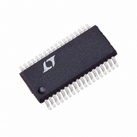
LTC3719EG Linear Technology, LTC3719EG Datasheet - Page 25

LTC3719EG
Manufacturer Part Number
LTC3719EG
Description
IC SW REG SYNC STEP-DOWN 36-SSOP
Manufacturer
Linear Technology
Datasheet
1.LTC3719EG.pdf
(32 pages)
Specifications of LTC3719EG
Applications
Controller, AMD Opteron™
Voltage - Input
4 ~ 36 V
Number Of Outputs
1
Voltage - Output
0.8 ~ 1.55 V
Operating Temperature
-40°C ~ 85°C
Mounting Type
Surface Mount
Package / Case
36-SSOP
Lead Free Status / RoHS Status
Contains lead / RoHS non-compliant
Available stocks
Company
Part Number
Manufacturer
Quantity
Price
Part Number:
LTC3719EG
Manufacturer:
LINEAR/凌特
Quantity:
20 000
Part Number:
LTC3719EG#PBF
Manufacturer:
LT/凌特
Quantity:
20 000
Company:
Part Number:
LTC3719EG#TR
Manufacturer:
LT
Quantity:
2 300
Part Number:
LTC3719EG#TRPBF
Manufacturer:
LINEAR/凌特
Quantity:
20 000
APPLICATIO S I FOR ATIO
Using Figure 4, the RMS ripple current will be:
An input capacitor(s) with a 5A
required.
The output capacitor ripple current is calculated by using
the inductor ripple already calculated for each inductor
and multiplying by the factor obtained from Figure 3
along with the calculated duty factor. The output ripple in
continuous mode will be highest at the maximum input
voltage since the duty factor is < 50%. The maximum
output current ripple is:
PC Board Layout Checklist
When laying out the printed circuit board, the following
checklist should be used to ensure proper operation of the
LTC3719. Check the following in your layout:
1) Are the signal and power grounds separate? The signal
ground traces should return to Pin 9 first. Connect Pin 9
to Pin 28 through a wide and straight trace. Then the signal
I
V
INRMS
OUTRIPPLE
I
I
COUT
COUTMAX
= (20A)(0.25) = 5A
V
OUT
fL
2
20
300
A
U
m
P P
0 5
-
.
kHz
1 2
at
2
.
U
A
V
24
P P
1 0
RMS
-
.
%
RMS
TRACE TO INDUCTOR
D F
H
ripple current rating is
40
W
0 5
.
mV
Figure 8. Proper Current Sense Connections
P P
-
U
PADS OF SENSE RESISTOR
SENSE
+
SENSE
ground joins the power ground plane beside Pin 28. It is
recommended that the Pin 28 return to the (–) plates of C
2) Does the LTC3719 V
load? Does the LTC3719 V
return?
3) Are the SENSE
minimum PC trace spacing? The filter capacitors between
SENSE
possible to the LTC3719. Ensure accurate current sensing
with Kelvin connections at the current sense resistor. See
Figure 8.
4) Does the (+) plate of C
topside MOSFETs as closely as possible? This capacitor
provides the AC current to the MOSFETs. Keep the input
current path formed by the input capacitor, top and bottom
MOSFETs, and the Schottky diode on the same side of the
PC board in a tight loop to minimize conducted and
radiated EMI.
5) Is the INTV
nected closely between INTV
capacitor carries the MOSFET driver peak currents. A
small value is recommended to allow placement immedi-
ately adjacent to the IC.
6) Keep the switching nodes, SW1 (SW2), away from
sensitive small-signal nodes. Ideally the switch nodes
should be placed at the furthest point from the
LTC3719.
7) Use a low impedance source such as a logic gate to drive
the PLLIN pin and keep the lead as short as possible.
–
TRACE TO OUTPUT CAP (+)
+
and SENSE
3719 F09
CC
–
1 F ceramic decoupling capacitor con-
and SENSE
–
pin pairs should be as close as
OS
IN
+
OS
connect to the drains of the
pin connect to the point of
CC
+
–
leads routed together with
and the PGND pin? This
pin connect to the load
LTC3719
sn3719 3719fs
25
IN
.


