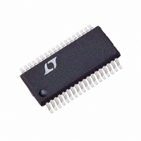
LTC3719EG Linear Technology, LTC3719EG Datasheet - Page 18

LTC3719EG
Manufacturer Part Number
LTC3719EG
Description
IC SW REG SYNC STEP-DOWN 36-SSOP
Manufacturer
Linear Technology
Datasheet
1.LTC3719EG.pdf
(32 pages)
Specifications of LTC3719EG
Applications
Controller, AMD Opteron™
Voltage - Input
4 ~ 36 V
Number Of Outputs
1
Voltage - Output
0.8 ~ 1.55 V
Operating Temperature
-40°C ~ 85°C
Mounting Type
Surface Mount
Package / Case
36-SSOP
Lead Free Status / RoHS Status
Contains lead / RoHS non-compliant
Available stocks
Company
Part Number
Manufacturer
Quantity
Price
Part Number:
LTC3719EG
Manufacturer:
LINEAR/凌特
Quantity:
20 000
Part Number:
LTC3719EG#PBF
Manufacturer:
LT/凌特
Quantity:
20 000
Company:
Part Number:
LTC3719EG#TR
Manufacturer:
LT
Quantity:
2 300
Part Number:
LTC3719EG#TRPBF
Manufacturer:
LINEAR/凌特
Quantity:
20 000
APPLICATIO S I FOR ATIO
LTC3719
Output Voltage
The LTC3719 has a true remote voltage sense capablity.
The sensing connections should be returned from the load
back to the differential amplifier’s inputs through a com-
mon, tightly coupled pair of PC traces. The differential
amplifier corrects for DC drops in both the power and
ground paths. The differential amplifier output signal is
divided down and compared with the internal precision
0.6V voltage reference by the error amplifier.
Output Voltage Programming
The output voltage is digitally programmed as defined in
Table 1 using the VID0 to VID4 logic input pins. The VID
logic inputs program a precision, 0.25% internal feedback
resistive divider. The LTC3719 has an output voltage range
of 0.8V to 1.55V in 25mV steps.
Between the ATTENOUT pin and ground is a variable
resistor, R1, whose value is controlled by the five VID input
pins (VID0 to VID4). Another resistor, R2, between the
ATTENIN and the ATTENOUT pins completes the resistive
divider. The output voltage is thus set by the ratio of
(R1 + R2) to R1.
Each VID digital input is pulled up by a 40k resistor in series
with a diode from V
get a digital low input, and can be either floated or con-
nected to V
is used to prevent the digital inputs from being damaged
or clamped if they are driven higher than V
inputs accept CMOS voltage levels.
V
normally connected to INTV
other sources. If it is driven from another source, that
source must be in the range of 2.7V to 5.5V and must be
alive prior to enabling the LTC3719.
18
BIAS
is the supply voltage for the VID section. It is
BIAS
to get a digital high input. The series diode
BIAS
U
. Therefore, it must be grounded to
U
CC
but can be driven from
W
BIAS
. The digital
U
Table 1. VID Output Voltage Programming
00000
00001
00010
00011
00100
00101
00110
00111
01000
01001
01010
01011
01100
01101
01110
01111
10000
10001
10010
10011
10100
10101
10110
10111
11000
11001
11010
11011
11100
11101
11110
11111
CODE
VID4
GND
GND
GND
GND
GND
GND
GND
GND
GND
GND
GND
GND
GND
GND
GND
GND
Float
Float
Float
Float
Float
Float
Float
Float
Float
Float
Float
Float
Float
Float
Float
Float
VID3
GND
GND
GND
GND
GND
GND
GND
GND
Float
Float
Float
Float
Float
Float
Float
Float
GND
GND
GND
GND
GND
GND
GND
GND
Float
Float
Float
Float
Float
Float
Float
Float
VID2
GND
GND
GND
GND
Float
Float
Float
Float
GND
GND
GND
GND
Float
Float
Float
Float
GND
GND
GND
GND
Float
Float
Float
Float
GND
GND
GND
GND
Float
Float
Float
Float
VID1
GND
GND
Float
Float
GND
GND
Float
Float
GND
GND
Float
Float
GND
GND
Float
Float
GND
GND
Float
Float
GND
GND
Float
Float
GND
GND
Float
Float
GND
GND
Float
Float
VID0
GND
Float
GND
Float
GND
Float
GND
Float
GND
Float
GND
Float
GND
Float
GND
Float
GND
Float
GND
Float
GND
Float
GND
Float
GND
Float
GND
Float
GND
Float
GND
Float
Shutdown
sn3719 3719fs
OUTPUT
1.550
1.525
1.500
1.475
1.450
1.425
1.400
1.375
1.350
1.325
1.300
1.275
1.250
1.225
1.200
1.175
1.150
1.125
1.100
1.075
1.050
1.025
1.000
0.975
0.950
0.925
0.900
0.875
0.850
0.825
0.800


