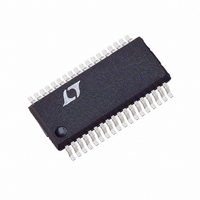
LTC3719EG Linear Technology, LTC3719EG Datasheet - Page 23

LTC3719EG
Manufacturer Part Number
LTC3719EG
Description
IC SW REG SYNC STEP-DOWN 36-SSOP
Manufacturer
Linear Technology
Datasheet
1.LTC3719EG.pdf
(32 pages)
Specifications of LTC3719EG
Applications
Controller, AMD Opteron™
Voltage - Input
4 ~ 36 V
Number Of Outputs
1
Voltage - Output
0.8 ~ 1.55 V
Operating Temperature
-40°C ~ 85°C
Mounting Type
Surface Mount
Package / Case
36-SSOP
Lead Free Status / RoHS Status
Contains lead / RoHS non-compliant
Available stocks
Company
Part Number
Manufacturer
Quantity
Price
Part Number:
LTC3719EG
Manufacturer:
LINEAR/凌特
Quantity:
20 000
Part Number:
LTC3719EG#PBF
Manufacturer:
LT/凌特
Quantity:
20 000
Company:
Part Number:
LTC3719EG#TR
Manufacturer:
LT
Quantity:
2 300
Part Number:
LTC3719EG#TRPBF
Manufacturer:
LINEAR/凌特
Quantity:
20 000
APPLICATIO S I FOR ATIO
Other “hidden” losses such as copper trace and internal
battery resistances can account for an additional 5% to
10% efficiency degradation in portable systems. It is very
important to include these “system” level losses in the
design of a system. The internal battery and input fuse
resistance losses can be minimized by making sure that
C
the switching frequency. A 50W supply will typically
require a minimum of 200 F to 300 F of output capaci-
tance having a maximum of 10m to 20m of ESR. The
LTC3719 2-phase architecture typically halves the input
and output capacitance requirements over competing
solutions. Other losses including Schottky conduction
losses during dead-time and inductor core losses gener-
ally account for less than 2% total additional loss.
Checking Transient Response
The regulator loop response can be checked by looking at
the load transient response. Switching regulators take
several cycles to respond to a step in DC (resistive) load
current. When a load step occurs, V
amount equal to I
series resistance of C
discharge C
forces the regulator to adapt to the current change and
return V
time V
ringing, which would indicate a stability problem. The
availability of the I
control loop behavior but also provides a DC coupled and
AC filtered closed loop response test point. The DC step,
rise time, and settling at this test point truly reflects the
closed loop response. Assuming a predominantly second
IN
has adequate charge storage and a very low ESR at
OUT
OUT
can be monitored for excessive overshoot or
OUT
to its steady-state value. During this recovery
generating the feedback error signal that
TH
LOAD
U
OUT
pin not only allows optimization of
(ESR), where ESR is the effective
( I
U
LOAD
) also begins to charge or
W
OUT
shifts by an
U
order system, phase margin and/or damping factor can be
estimated using the percentage of overshoot seen at this
pin. The bandwidth can also be estimated by examining
the rise time at the pin. The I
shown in the Figure 1 circuit will provide an adequate
starting point for most applications.
The I
loop compensation. The values can be modified slightly
(from 0.2 to 5 times their suggested values) to optimize
transient response once the final PC layout is done and the
particular output capacitor type and value have been
determined. The output capacitors need to be decided
upon first because the various types and values determine
the loop gain and phase. An output current pulse of 20%
to 80% of full-load current having a rise time of <2 s will
produce output voltage and I
give a sense of the overall loop stability without breaking
the feedback loop. The initial output voltage step resulting
from the step change in output current may not be within
the bandwidth of the feedback loop, so this signal cannot
be used to determine phase margin. This is why it is
better to look at the Ith pin signal which is in the feedback
loop and is the filtered and compensated control loop
response. The gain of the loop will be increased by
increasing R
increased by decreasing C
same factor that C
be kept the same, thereby keeping the phase the same in
the most critical frequency range of the feedback loop.
The output voltage settling behavior is related to the
stability of the closed-loop system and will demonstrate
the actual overall supply performance.
TH
series R
C
and the bandwidth of the loop will be
C
-C
C
is decreased, the zero frequency will
C
filter sets the dominant pole-zero
C
. If R
TH
TH
pin waveforms that will
C
external components
is increased by the
LTC3719
sn3719 3719fs
23


