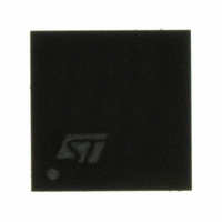
PM6685 STMicroelectronics, PM6685 Datasheet - Page 43

PM6685
Manufacturer Part Number
PM6685
Description
IC CTLR DUAL SYNC STDN 5X5VFQFPN
Manufacturer
STMicroelectronics
Specifications of PM6685
Applications
Controller, Notebook Power System
Voltage - Input
6 ~ 28 V
Number Of Outputs
2
Voltage - Output
-3.3V, 5V
Operating Temperature
0°C ~ 85°C
Mounting Type
Surface Mount
Package / Case
32-VFQFN, 32-VFQFPN
Output Voltage
5 V, 3.3 V
Output Current
0.1 A
Input Voltage
5.5 V to 28 V
Mounting Style
SMD/SMT
Maximum Operating Temperature
+ 125 C
Minimum Operating Temperature
- 10 C
Lead Free Status / RoHS Status
Lead free / RoHS Compliant
Available stocks
Company
Part Number
Manufacturer
Quantity
Price
Company:
Part Number:
PM6685
Manufacturer:
RENESAS
Quantity:
1 370
Part Number:
PM6685
Manufacturer:
ST
Quantity:
20 000
Part Number:
PM6685TR
Manufacturer:
ST
Quantity:
20 000
PM6685
10.8
OUT3: The ripple is greater than 30 mV, then the virtual ESR network is not required.
C
Layout guidelines
The layout is very important in terms of efficiency, stability and noise of the system. It is
possible to refer to the PM6685 demonstration board for a complete layout example.
For good PC board layout follows these guidelines:
●
●
●
●
INT
Place on the top side all the power components (inductors, input and output capacitors,
MOSFETs and diodes). Refer them to a power ground plan, PGND. If possible, reserve
a layer to PGND plan. The PGND plan is the same for both the switching sections.
AC current paths layout is very critical (see
minimize their length. Trace the LS MOSFET connection to PGND plan as short as
possible. Place the synchronous diode D near the LS MOSFET. Connect the LS
MOSFET drain to the switching node with a short trace.
Place input capacitors near HS MOSFET drain. It is recommended to use the same
input voltage plan for both the switching sections, in order to put together all input
capacitors.
Place all the sensitive analog signals (feedbacks, voltage reference, current sense
paths) on the bottom side of the board or in an inner layer. Isolate them from the power
top side with a signal ground layer, SGND. Connect the SGND and PGND plans only in
one point (a multiple vias connection is preferable to a 0 ohm resistor connection) near
the PGND device pin. Place the device on the top or on the bottom size and connect
the exposed pad and the SGND pins to the SGND plan (see
=1 nF; C
filt
= 47 pF; R
INT
Doc ID 11674 Rev 8
= 1 kΩ
Figure 41 on page 44
Figure 41 on page 44
). The first priority is to
Design example
43/48
).


