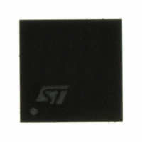
PM6685 STMicroelectronics, PM6685 Datasheet - Page 7

PM6685
Manufacturer Part Number
PM6685
Description
IC CTLR DUAL SYNC STDN 5X5VFQFPN
Manufacturer
STMicroelectronics
Specifications of PM6685
Applications
Controller, Notebook Power System
Voltage - Input
6 ~ 28 V
Number Of Outputs
2
Voltage - Output
-3.3V, 5V
Operating Temperature
0°C ~ 85°C
Mounting Type
Surface Mount
Package / Case
32-VFQFN, 32-VFQFPN
Output Voltage
5 V, 3.3 V
Output Current
0.1 A
Input Voltage
5.5 V to 28 V
Mounting Style
SMD/SMT
Maximum Operating Temperature
+ 125 C
Minimum Operating Temperature
- 10 C
Lead Free Status / RoHS Status
Lead free / RoHS Compliant
Available stocks
Company
Part Number
Manufacturer
Quantity
Price
Company:
Part Number:
PM6685
Manufacturer:
RENESAS
Quantity:
1 370
Part Number:
PM6685
Manufacturer:
ST
Quantity:
20 000
Part Number:
PM6685TR
Manufacturer:
ST
Quantity:
20 000
PM6685
Table 2.
Pin
19
20
21
22
23
24
25
26
27
28
29
30
31
32
33
CSENSE5
LDO3SEL
PGOOD5
PGOOD3
EXP PAD
PHASE5
HGATE5
COMP5
BOOT5
Name
OUT5
VREF
SKIP
VCC
EN5
VIN
Pin functions (continued)
Device input supply voltage. A bypass filter (4W and 4.7mF) between the battery and this pin is
recommended.
Current sense input for the 5V section. This pin must be connected through a resistor to the
drain of the synchronous rectifier (R
Switch node connection and return path for the high side driver for the 5V section.
High-side gate driver output for the 5V section.
Bootstrap capacitor connection for the 5V section. It supplies the high-side gate driver.
Pulse skip mode control input.
– If the pin is connected to LDO5 the PWM mode is enabled.
– If the pin is connected to GND, the pulse skip mode is enabled.
– If the pin is connected to VREF the pulse skip mode is enabled but the switching frequency is
5V SMPS enable input.
– The 5V section is enabled applying a voltage greater than 2.4V to this pin.
– The 5V section is disabled applying a voltage lower than 0.8V.
When the section is disabled the High Side gate driver goes low and Low Side gate driver goes
high.
Power Good signal for the 5V section. This pin is an open drain output.
The pin is pulled low if the output is disabled or if it is out of approximately +/- 10% of its nominal
value.
Power Good signal for the 3.3V section. This pin is an open drain output.
The pin is pulled low if the output is disabled or if it is out of approximately +/- 10% of its nominal
value.
Control pin for the 3.3V internal linear regulator. This pin determines three operative modes for
the LDO3.
– If LDO3_SEL pin is connected to GND the LDO3 output is always disabled.
– If LDO3_SEL pin is connected to LDO5 the LDO3 internal regulator is always enabled.
– If LDO3_SEL pin is connected to VREF and OUT3 is greater than about 3V, the LDO3
Output voltage sense for the 5V switching section.This pin must be directly connected to the
output voltage of the switching section.
DC voltage error compensation pin for the 5V switching section.
Device Supply Voltage pin. It supplies the all the internal analog circuitry except the gate drivers
(see LDO5). Connect this pin to LDO5.
High accuracy output voltage reference (1.230V). It can deliver 50uA. Bypass to SGND with a
100nF capacitor.
Exposed pad.
kept higher than 33kHz (No-audible pulse skip mode).
regulator shuts down and the LDO3 pin is be directly connected to OUT3 through a 3W (max)
switch.
Doc ID 11674 Rev 8
DSON
Description
sensing) to set the current limit threshold.
Pin settings
7/48


