ISL6444CA Intersil, ISL6444CA Datasheet
ISL6444CA
Specifications of ISL6444CA
Available stocks


Related parts for ISL6444CA

ISL6444CA Summary of contents
Page 1
... Routers and Switchers Ordering Information PART NUMBER ISL6444CA* ISL6444CAZ* (Note) *Add “-T” suffix for tape and reel. NOTE: Intersil Pb-free plus anneal products employ special Pb-free material sets; molding compounds/die attach materials and 100% matte tin plate termination finish, which are RoHS compliant and compatible with both SnPb and Pb-free soldering operations ...
Page 2
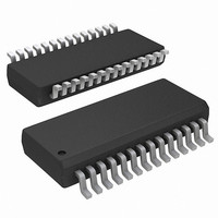
Pinout ISL6444 (28 LD QSOP) TOP VIEW 1 GND LGATE1 2 PGND1 3 PHASE1 4 5 UGATE1 BOOT1 6 ISEN1 7 8 EN1 9 VOUT1 VSEN1 10 OCSET1 11 12 SOFT1 13 DDR 14 VIN Generic Application Circuits OCSET1 OCSET2 ...
Page 3
Generic Application Circuits +5V DDR OCSET1 V OUT3 DDR REF (+1.25V) PGOOD2/REF ISL6444 APPLICATION CIRCUIT FOR COMPLETE DDR MEMORY POWER SUPPLY 3 ISL6444 (Continued) +V +5V...24V PWM1 Q2 C1 OCSET2 PWM2 V OUT1 VDDQ (+2.5V ...
Page 4
Absolute Maximum Ratings Bias Voltage ...
Page 5
Electrical Specifications Recommended Operating Conditions, Unless Otherwise Noted. (Continued) PARAMETER Undervoltage Shut-Down Level Overvoltage Shut-Down GATE DRIVERS Upper Drive Pull-Up Resistance Upper Drive Pull-Down Resistance Lower Drive Pull-Up Resistance Lower Drive Pull-Down Resistance POWER GOOD AND CONTROL FUNCTIONS Power Good ...
Page 6
Block Diagram BOOT1 UGATE1 UG1 HI OVP1 PHASE1 GATE GATE LOGIC CONTROL VCC LG1 LGATE1 LO OVP1 PGND1 MODE CHANGE COMP 1 - HYST COMP 1 - EA1 VSEN1 - - Σ VREF LGATE1 LGATE1 ISEN1 CSA1 - VSEN1 OVP1 ...
Page 7
Functional Pin Description GND (Pin 1) Signal ground for the IC. LGATE1, LGATE2 (Pin 2, 27) These are outputs of the lower MOSFET drivers. PGND1, PGND2 (Pin 3, 26) These pins provide the return connection for lower gate drivers. These ...
Page 8
Description Operation The ISL6444 is a dual channel PWM controller intended for use in power supplies for graphic chipset, SDRAM, DDR DRAM or other low voltage power applications in modern notebook and sub-notebook PCs. The IC integrates two control circuits ...
Page 9
MOSFET compared to a Shottky diode. In contrast, continuous-conduction operation in load currents lower than the inductor critical value results in lower efficiency. In this case, during a fraction of a switching cycle, the direction of the inductor current ...
Page 10
VOUT pin and Forced Continuous Conduction Mode (FCCM) The error amplifier that provides control over the converter during CCM mode is excluded from the ...
Page 11
Gate Control Logic The gate control logic translates generated PWM signals into gate drive signals providing necessary amplification, level shift, and shoot-trough protection. Also, it bears some functions that help to optimize the IC performance over a wide range of ...
Page 12
Overtemperature Protection The chip incorporates an over temperature protection circuit that shuts the chip down when the die temperature of +150°C is reached. Normal operation restores at die temperatures below +125°C through the full soft-start cycle. DDR Application Double Data ...
Page 13
In the case when power for VDDQ is taken from the +5V system rail, as Figure 8 shows, both in-phase and out-of- phase approaches are susceptible to noise in the sourcing mode. 300kHz CLOCK VDDQ SOURCING VTT OUT-OF-PHASE SINKING SOURCING ...
Page 14
... Figure 13 depicts the DDR solution in the case where the 5V system rail is used as a primary voltage source. For detailed information on the circuit, including a Bill-of- Materials and circuit board description, see Application Note AN9995. Also see Intersil’s web site (http://www.intersil.com) for the latest information 1μ ...
Page 15
C1 C3 CR1 1μF 0.01μF Q1 1/2 IRF7313 C6 UGATE1 0.1μF PHASE1 L1 +V2_5S 4.7μH R1 (3A 330μF LGATE1 Q2 R3 2/2 IRF7313 R5 R7 FIGURE 10. DUAL OUTPUT APPLICATION CIRCUIT FOR TWO-STEP CONVERSION 15 ISL6444 R9 ...
Page 16
C1 10μF C3 CR1 0.01μF SOFT1 BOOT1 Q1 1/2 IRF7313 C6 UGATE1 0.1μF PHASE1 L1 10.0μH R1 ISEN1 330μF LGATE1 Q2 R3 2/2 IRF7313 6.89k PGND1 VSEN1 VOUT1 R5 10k EN1 PG1 OCSET1 R7 R9 0.01 C10 ...
Page 17
CR1 Q1 1/2 IRF7313 C6 0.1μF VDDQ L1 +2.5V 4.7μH (6A 330μ 2/2 IRF7313 32k4 R4 18k2 R5 18k2 R6 C10 18k2 0.01μF FIGURE 12. APPLICATION CIRCUIT FOR COMPLETE DDR MEMORY POWER SOLUTION WITH ONE-STEP CONVERSION ...
Page 18
C1 10μF CR1 0.01μF Q1 1/2 IRF7313 C6 0.1μF VDDQ L1 +2.5V 4.7μH R1 (6A 330μ 2/2 IRF7313 32k4 R4 18k2 R7 R5 18k2 R6 C10 18k2 0.01μF FIGURE 13. APPLICATION CIRCUIT FOR COMPLETE ...
Page 19
... Accordingly, the reader is cautioned to verify that data sheets are current before placing orders. Information furnished by Intersil is believed to be accurate and reliable. However, no responsibility is assumed by Intersil or its subsidiaries for its use; nor for any infringements of patents or other rights of third parties which may result from its use ...