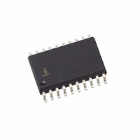
EL7571CMZ Intersil, EL7571CMZ Datasheet - Page 3

EL7571CMZ
Manufacturer Part Number
EL7571CMZ
Description
IC CTRLR PWM PROGRAMMABLE 20SOIC
Manufacturer
Intersil
Datasheet
1.EL7571CM.pdf
(19 pages)
Specifications of EL7571CMZ
Applications
Controller, Intel Pentium® II, Pro
Voltage - Input
4.5 ~ 12.6 V
Number Of Outputs
2
Voltage - Output
1.3 ~ 3.5 V
Operating Temperature
0°C ~ 70°C
Mounting Type
Surface Mount
Package / Case
20-SOIC (7.5mm Width)
Lead Free Status / RoHS Status
Lead free / RoHS Compliant
Pin Descriptions
NOTE: Pin designators: I = Input, O = Output, S = Supply
DC Electrical Specifications
AC Electrical Specifications
I
I
f
f
t
t
T
D
VID
OTEN
OSC
CLK
OTEN
SYNC
PIN NO.
START
MAX
PARAMETER
PARAMETER
10
11
12
13
14
15
16
17
18
19
20
1
2
3
4
5
6
7
8
9
PIN NAME
CSLOPE
PWRGD
COSC
GNDP
OTEN
VINP
VID0
VID1
VID2
VID3
VID4
GND
REF
HSD
LSD
VH1
VIN
CS
FB
LX
VID Input Pull up Current
OTEN Input Pull up Current
Nominal Oscillator Frequency
Clock Frequency
Shutdown Delay
Oscillator Sync. Pulse Width
Soft-start Period
Maximum Duty Cycle
PIN TYPE
(NOTE 1)
O
O
O
O
S
S
S
S
S
S
I
I
I
I
I
I
I
I
I
I
DESCRIPTION
3
DESCRIPTION
Chip enable input, internal pull up (5mA typical). Active high.
With a capacitor attached from CSLOPE to GND, generates the voltage ramp compensation for the PWM
current mode controller. Slope rate is determined by an internal 14uA pull up and the C
value. VC
Multi-function pin: with a timing capacitor attached, sets the internal oscillator rate f
when pulsed low for a duration t
Band gap reference output. Decouple to GND with 0.1uF.
Power good, open drain output. Set low whenever the output voltage is not within ±13% of the programmed
value.
Bit 0 of the output voltage select DAC. Internal pull up sets input high when not driven.
Bit 1 of the output voltage select DAC. Internal pull up sets input high when not driven.
Bit 2 of the output voltage select DAC. Internal pull up sets input high when not driven.
Bit 3 of the output voltage select DAC. Internal pull up sets input high when not driven.
Bit 4 of the output voltage select DAC. Internal pull up sets input high when not driven.
Voltage regulation feedback input. Tie to V
Current sense. Current feedback input of PWM controller and over current capacitor input. Current limit
threshold set at +154mV with respect to FB. Connect sense resistor between CS and FB for normal
operation.
Ground
Power ground for low side FET driver. Tie to GND for normal operation.
Low side gate drive output.
Input supply voltage for low side FET driver. Tie to VIN for normal operation.
Input supply voltage for control unit.
Negative supply input for high side FET driver.
High side gate drive output. Driver ground referenced to LX. Driver supply may be bootstrapped to enhance
low controller input voltage operation.
Positive supply input for high side FET driver.
T
T
(Continued)
A
A
= 25°C, V
= 25°C, V
SLOPE
IN
IN
is reset to ground at the termination of the high side cycle.
= 5V, C
= 5V, C
OSC
OSC
C
V
Oscillator i/p (COSC) driven with
HCMOS gate
V
OTEN
OUT
OSC
EL7571
= 330pF, C
= 330pF, C
= 3.5V
SYNC
= 330pF
>1.5V
CONDITION
CONDITIONS
synchronizes device to an external clock.
SLOPE
SLOPE
OUT
FUNCTION
for normal operation.
= 390pF, R
= 390pF unless otherwise specified.
SENSE
MIN
MIN
= 7.5mΩ unless otherwise specified.
140
3
3
50
20
100/f
TYP
TYP
190
500
100
97
5
5
CLK
S
(kHz) = 57/C
SLOPE
MAX
MAX
1000
240
800
7
7
capacitor
OSC
UNIT
UNIT
kHz
kHz
µA
µA
ns
ns
us
%
(µF);


