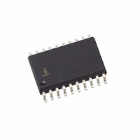
EL7571CMZ Intersil, EL7571CMZ Datasheet - Page 8

EL7571CMZ
Manufacturer Part Number
EL7571CMZ
Description
IC CTRLR PWM PROGRAMMABLE 20SOIC
Manufacturer
Intersil
Datasheet
1.EL7571CM.pdf
(19 pages)
Specifications of EL7571CMZ
Applications
Controller, Intel Pentium® II, Pro
Voltage - Input
4.5 ~ 12.6 V
Number Of Outputs
2
Voltage - Output
1.3 ~ 3.5 V
Operating Temperature
0°C ~ 70°C
Mounting Type
Surface Mount
Package / Case
20-SOIC (7.5mm Width)
Lead Free Status / RoHS Status
Lead free / RoHS Compliant
Converter Topologies
Modern logic level power FET’s rapidly increase in resistivity
(R
thermal damage to the power FET’s under load, with a
reduced supply voltage, the system watchdog monitors the
controller supply (V
(HSD, LSD) when the supply voltage drops below 3.5V.
When the supply voltage is increased above 4V the
watchdog initiates a soft-start ramp and enables PWM
operation. The difference between enable and disable
thresholds introduces hysteresis into the circuit operation,
preventing start-up oscillation. In addition, output voltage is
also monitored by the watchdog. As called out by the Intel
Pentium® II VRM specification, the watchdog power good
output (PWRGD) is set low whenever the output voltage
differs from it’s selected value by more than ±13%. PWRGD
is an open drain output. A third watchdog function disables
PWM output switching during over-voltage fault conditions,
displaying both external FET drives, whenever the output
voltage is greater than 13% of its selected value, thereby
anticipating reverse inductor current ramping and
conforming to the VRM over-voltage specification, which
requires the regulator output to be disabled during fault
conditions. Switching is enabled after the fault condition is
removed.
Output Drivers
Complementary control signals developed by the PWM
control loop are fed to dual NMOS power FET drivers via a
Circuit schematics and Bills of Material (BOMs) for the
various topologies are provided at the end of this data sheet.
If your application requirements differ from the included
samples, the following design guide lines should be used to
select the key component values. Refer to the front page
connection diagram for component locations.
Output Inductor, L
Two key converter requirements are used to determine
inductor value:
• I
• I
5V only Non-synchronous
5V only Synchronous
5V &12V Non-synchronous
5V & 12V Synchronous
12V only Synchronous
DS-ON
the converter enters the discontinuous mode of operation
(refer to Elantec application note #18 for a detailed
discussion of discontinuous mode)
MIN
MAX
- minimum output current; the current level at which
- maximum output current
) as their gate drive is reduced below 5V. To prevent
TOPOLOGY
IN
) and disables both PWM outputs
1
8
Connection Diagram
DIAGRAM
figure 1
figure 2
figure 3
figure 4
EFFICIENCY
EL7571
92%
95%
92%
95%
92%
level shift circuit. Each driver is capable of delivering nominal
peak output currents of 2A at 12V. To prevent shoot-through
in the external FET’s, each driver is disabled until the gate
voltage of the complementary power FET has fallen to less
than 1V. Supply connections for both drivers are
independent, allowing the controller to be configured with a
boot-strapped high side drive. Employing this technique a
single supply voltage may be used for both power FET’s and
controller. Alternatively, the application may be simplified
using dual supply rails with the power FET’s connected to a
secondary supply voltage below the controller’s, typically
12V and 5V. For applications where efficiency is less
important than cost, applications can be further simplified by
replacing the low side power FET with a Schottky diode,
resulting in non-synchronous operation.
Applications Information
The EL7571 is designed to meet the Intel 5 bit VRM
specification. Refer to the VID decode table for the controller
output voltage range.
The EL7571 may be used in a number converter topologies.
The trade-off between efficiency, cost, circuit complexity, line
input noise, transient response and availability of input
supply voltages will determine which converter topology is
suitable for a given application. The following table lists some
of the differences between the various configurations:
Although many factors influence the choice of the inductor
value, including efficiency, transient response and ripple
current, one practical way of sizing the inductor is to select a
value which maintains continuous mode operation, i.e.
inductor current positive for all conditions. This is desirable to
optimize load regulation and light load transient response.
When the minimum inductor ripple current just reaches zero
and with the mean ripple current set to I
ripple current is twice I
minimum inductor value is given by:
highest
L
lowest
COST
higher
high
1MIN
low
=
(
------------------------------------------------------- -
V
IN
COMPLEXITY INPUT NOISE
–
highest
higher
lowest
V
1
high
PEAK
low
OUT
MAX
)
, independent of duty cycle. The
×
T
ON
=
high
high
high
high
high
(
----------------------------------------------------------- -
V
V
IN
IN
MIN
×
–
F
V
SW
, peak inductor
OUT
×
TRANSIENT
RESPONSE
)
2
×
×
good
good
good
good
V
best
I
OUT
MIN


