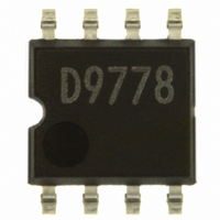
BD9778F-E2 Rohm Semiconductor, BD9778F-E2 Datasheet - Page 11

BD9778F-E2
Manufacturer Part Number
BD9778F-E2
Description
IC REG SW 2A P-CH MOSF STDN SOP8
Manufacturer
Rohm Semiconductor
Type
Step-Down (Buck)r
Specifications of BD9778F-E2
Internal Switch(s)
Yes
Synchronous Rectifier
No
Number Of Outputs
1
Voltage - Output
1 ~ 35 V
Current - Output
2A
Frequency - Switching
50kHz ~ 500kHz
Voltage - Input
7 ~ 35 V
Operating Temperature
-40°C ~ 125°C
Mounting Type
Surface Mount
Package / Case
8-SOP
Power - Output
690mW
No. Of Outputs
1
Output Voltage
35V
Output Current
2A
Voltage Regulator Case Style
SOP
No. Of Pins
8
Operating Temperature Range
-40°C To +125°C
Svhc
No SVHC (18-Jun-2010)
Base Number
9778
Input Voltage
35 V
Switching Frequency
102 KHz
Mounting Style
SMD/SMT
Lead Free Status / RoHS Status
Lead free / RoHS Compliant
Lead Free Status / RoHS Status
Lead free / RoHS Compliant, Lead free / RoHS Compliant
Other names
BD9778F-E2TR
Available stocks
Company
Part Number
Manufacturer
Quantity
Price
Company:
Part Number:
BD9778F-E2
Manufacturer:
SHARP
Quantity:
1 000
Part Number:
BD9778F-E2
Manufacturer:
ROHM/罗姆
Quantity:
20 000
1.
※ As shown above, design the GND pattern as large area as possible
※ Gray zones indicate GND.
within inner layer.
Phase compensation setting procedure
The following section describes the stability conditions of the negative feedback system.
Since the DC/DC converter application is sampled according to the switching frequency, GBW (frequency at 0-dB gain)
of the overall system should be set to 1/10 or less of the switching frequency. The following section summarizes the targeted
characteristics of this application.
・ At a 1 (0-dB) gain, the phase delay is 150˚ or less (i.e., the phase margin is 30˚ or more).
・ The GBW for this occasion is 1/10 or less of the switching frequency.
Responsiveness is determined with restrictions on the GBW. To improve responsiveness, higher switching frequency
should be provided.
Replace a secondary phase delay (-180˚) with a secondary phase lead by inserting two phase leads, to ensure the stability
through the phase compensation. Furthermore, the GBW (i.e., frequency at 0-dB gain) is determined according to phase
compensation capacitance provided for the error amplifier. Consequently, in order to reduce the GBW,
increase the capacitance value.
Application stability conditions
※Oscillation frequency s graph value is Typical value,
Fig.32 BD9001F reference layout pattern
oscillation frequency is necessary to consider
Fig.34 R
(1) Typical integrator (Low pass filter)
Since the error amplifier is provided with (1) or (2) phase compensation, the low pass filter is applied. In the case of
the DC/DC converter application, the R becomes a parallel resistance of the feedback resistance.
OSCILATING FREQUENCY SETTING RESISTANCE : R
Co
500
450
400
350
300
250
200
150
100
50
T
0
vs f
Feedback
L
100
OSC
200
Cx2
C3
R2
(BD9781HFP/BD9778F/HFP)
300
Di
R1
R
400
500
600
-
A
700
C
C
±
20% as dispersion.
800
T
[kΩ]
FB
11/16
Fig.33 BD9781HFP reference layout pattern
(2) Open loop characteristics of integrator
Phase
Gain
[dB]
[˚]
OSCILATING FREQUENCY SETTING RESISTANCE : RT [kΩ]
-180
0
-90
A
0
C
300
250
200
150
100
50
Di
Fig.35 R
Point (a) fa =
Point (b) fa = GBW =
50
100
L
200
(a)
T
300
R
C
Co
vs f
T
T
-90˚
400
Cx1
OSC
2 RCA
-20dB/decade
500
1
Phase
margin
(BD9001F)
600
[Hz]
2 RC
700
1
GBW(b)
800
[Hz]
-180˚
f
f


