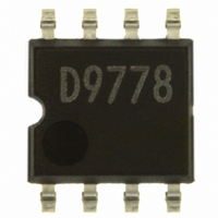
BD9778F-E2 Rohm Semiconductor, BD9778F-E2 Datasheet - Page 14

BD9778F-E2
Manufacturer Part Number
BD9778F-E2
Description
IC REG SW 2A P-CH MOSF STDN SOP8
Manufacturer
Rohm Semiconductor
Type
Step-Down (Buck)r
Specifications of BD9778F-E2
Internal Switch(s)
Yes
Synchronous Rectifier
No
Number Of Outputs
1
Voltage - Output
1 ~ 35 V
Current - Output
2A
Frequency - Switching
50kHz ~ 500kHz
Voltage - Input
7 ~ 35 V
Operating Temperature
-40°C ~ 125°C
Mounting Type
Surface Mount
Package / Case
8-SOP
Power - Output
690mW
No. Of Outputs
1
Output Voltage
35V
Output Current
2A
Voltage Regulator Case Style
SOP
No. Of Pins
8
Operating Temperature Range
-40°C To +125°C
Svhc
No SVHC (18-Jun-2010)
Base Number
9778
Input Voltage
35 V
Switching Frequency
102 KHz
Mounting Style
SMD/SMT
Lead Free Status / RoHS Status
Lead free / RoHS Compliant
Lead Free Status / RoHS Status
Lead free / RoHS Compliant, Lead free / RoHS Compliant
Other names
BD9778F-E2TR
Available stocks
Company
Part Number
Manufacturer
Quantity
Price
Company:
Part Number:
BD9778F-E2
Manufacturer:
SHARP
Quantity:
1 000
Part Number:
BD9778F-E2
Manufacturer:
ROHM/罗姆
Quantity:
20 000
Cautions on use
SW
SW
EN(BD9778F/HFP, BD9001F)
EN
1) Absolute maximum ratings
2) GND potential
3) Thermal design
4) Inter-pin shorts and mounting errors
5) Operation in strong electromagnetic field
6) Inspection with set printed circuit board
7) IC pin input (Fig. 37)
(Pin A)
P layer
An excess in the absolute maximum ratings, such as supply voltage, temperature range of operating conditions, etc., can break down
the devices, thus making impossible to identify breaking mode, such as a short circuit or an open circuit. If any over rated values will
expect to exceed the absolute maximum ratings, consider adding circuit protection devices, such as fuses. Furthermore, don't turn on
the IC with a fast rising edge of V
GND potential should maintain at the minimum ground voltage level. Furthermore, no terminals should be lower than the GND
potential voltage including an electric transients.
Use a thermal design that allows for a sufficient margin in light of the power dissipation (Pd) in actual operating conditions.
Use caution when positioning the IC for mounting on printed circuit boards. The IC may be damaged if there is any connection error or
if positive and ground power supply terminals are reversed. The IC may also be damaged if pins are shorted together or are shorted to
other circuits power lines.
Use caution when using the IC in the presence of a strong electromagnetic field as doing so may cause the IC to malfunction.
When testing the IC on an application board, connecting a capacitor to a pin with low impedance subjects the IC to stress.
Always discharge capacitors after each process or step. Always turn the IC's power supply off before connecting it to, or removing it
from a jig or fixture, during the inspection process. Ground the IC during assembly steps as an
Use similar precaution when transporting and storing the IC.
This monolithic IC contains P+ isolation and P substrate layers between adjacent elements to keep them isolated.
P-N junctions are formed at the intersection of these P layers with the N layers of other elements, creating a parasitic diode or transistor.
For example, the relation between each potential is as follows:
the IC. The operation of parasitic diodes can result in mutual interference among circuits, operational faults, or physical damage.
Accordingly, methods by which parasitic diodes operate, such as applying a voltage that is lower than the GND (P substrate) voltage to
an input pin, should not be used.
N
When GND > Pin A and GND > Pin B, the P-N junction operates as a parasitic diode.
When Pin B > GND > Pin A, the P-N junction operates as a parasitic transistor. Parasitic diodes can occur inevitably in the structure of
VIN
P +
VIN
10kΩ
300kΩ
250kΩ
Resistor
VIN
N
P
Parasitic element
GND
RT
RT
FB(BD9001F)
IN
P +
Fig.37 Typical simple construction of monolithic IC
. ( rise time << 10V / μsec )
FB
N
VIN
VIN
2kΩ
(Pin B)
1kΩ
VREF
N
Fig.36 Equivalent circuit
Parasitic element
300kΩ
P +
1kΩ
50kΩ
C
14/16
Transistor (NPN)
VREF
B
N
N
E
FB
P
GND
FB(BD9778F/HFP, BD9781HFP)
P layer
VIN
1kΩ
EN/SYNC(BD9781HFP)
P +
EN/SYNC
N
GND
VREF
VIN
antistatic measure.
222
145
kΩ
kΩ
(PIN B)
(Pin A)
INV
139
221
kΩ
kΩ
INV
GND
B
VIN
1kΩ
Parasitic element
VREGA
2kΩ
GND
Parasitic element
C
E
VREF


