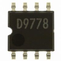
BD9778F-E2 Rohm Semiconductor, BD9778F-E2 Datasheet - Page 13

BD9778F-E2
Manufacturer Part Number
BD9778F-E2
Description
IC REG SW 2A P-CH MOSF STDN SOP8
Manufacturer
Rohm Semiconductor
Type
Step-Down (Buck)r
Specifications of BD9778F-E2
Internal Switch(s)
Yes
Synchronous Rectifier
No
Number Of Outputs
1
Voltage - Output
1 ~ 35 V
Current - Output
2A
Frequency - Switching
50kHz ~ 500kHz
Voltage - Input
7 ~ 35 V
Operating Temperature
-40°C ~ 125°C
Mounting Type
Surface Mount
Package / Case
8-SOP
Power - Output
690mW
No. Of Outputs
1
Output Voltage
35V
Output Current
2A
Voltage Regulator Case Style
SOP
No. Of Pins
8
Operating Temperature Range
-40°C To +125°C
Svhc
No SVHC (18-Jun-2010)
Base Number
9778
Input Voltage
35 V
Switching Frequency
102 KHz
Mounting Style
SMD/SMT
Lead Free Status / RoHS Status
Lead free / RoHS Compliant
Lead Free Status / RoHS Status
Lead free / RoHS Compliant, Lead free / RoHS Compliant
Other names
BD9778F-E2TR
Available stocks
Company
Part Number
Manufacturer
Quantity
Price
Company:
Part Number:
BD9778F-E2
Manufacturer:
SHARP
Quantity:
1 000
Part Number:
BD9778F-E2
Manufacturer:
ROHM/罗姆
Quantity:
20 000
V
SW
waveform
GND
IN
The heat loss W of the IC can be obtained by the formula shown below:
W=Ron × Io
Heat loss
For thermal design, be sure to operate the IC within the following conditions.
(Since the temperatures described hereunder are all guaranteed temperatures, take the margin into account.)
The chip junction temperature Tj can be considered in the following two patterns:
<Reference value> θj-c : HRP7
To obtain Tj from the IC surface
temperature Tc in the actual use state,
Ron: ON resistance of IC (refer to pages 4 and 5.) Io: Load current Vo: Output voltage
<Reference> Measurement of open loop of DC/DC converter
V
1. The ambient temperature Ta is to be 125˚C or less.
2. The chip junction temperature Tj is to be 150˚C or less.
Output voltage
Tr: Switching rise/fall time (Approximately 40 nsec)
IN
f : Oscillation frequency
Tj = T
: Input voltage Icc: Circuit current (Refer to pages 2 and 3)
Tr
DC/DC converter
Load
controller
To measure the open loop of DC/DC converter, use the gain phase analyzer or FRA to measure the frequency
characteristics.
0
C
2
+θj-c × W
×
V
Vo
IN
2
1
+ V
T =
SOP8 32.5˚C/W
IN
1
f
× I
Maximum load
CC
7˚C/W
+ Tr × V
+
Inadequate phase margin
Adequate phase margin
IN
V
~
V
O
m
× Io × f
<Reference value> θj-a : HRP7 89.3˚C/W
To obtain Tj from the ambient temperature Ta
R
L
Tj=Ta+θj-a × W
<Procedure>
r
t
13/16
1. Check to ensure output causes no oscillation at the maximum
2.
3.
Furthermore, the phase margin can also be measured with the
load responsiveness.
Measure variations in the output voltage when instantaneously
changing the load from no load to the maximum load.
Even though ringing phenomenon is caused, due to low phase margin,
no ringing takes place. Phase margin is provided. However,
no specific phase margin can be probed.
1 Ron X Io
2 2 X
SOP8 222.2˚C/W Single piece of IC
load in closed loop.
Isolate (1) and (2) and insert Vm (with amplitude of
approximately 100 mVpp).
Measure (probe) the oscillation of
=Tr X V
1
2
181.8˚C/W
54.3˚C/W
22.7˚C/W
PCB size: 70 × 70 × 1.6 mm
Copper foil area on the front side of PCB: 10.5 × 10.5 mm
PCB size: 70 × 70 × 1.6 mm
X Tr X
IN
2
X Io X f
1
T
X V
Single piece of IC
2-layer PCB (Copper foil area on the front side
of PCB: 15 × 15 mm
2-layer PCB (Copper foil area on the front side
of PCB: 70 × 70 mm
1-layer PCB
IN
X Io
A
3
3
(PCB incorporates thermal via.)
(1)
2
2
)
)
to that of (2).
2


