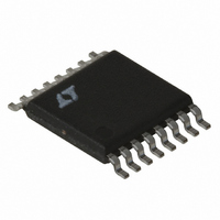
LT1766EFE#TRPBF Linear Technology, LT1766EFE#TRPBF Datasheet - Page 18

LT1766EFE#TRPBF
Manufacturer Part Number
LT1766EFE#TRPBF
Description
IC REG SW HV 1.5A 200KHZ 16TSSOP
Manufacturer
Linear Technology
Type
Step-Down (Buck)r
Datasheet
1.LT1766EGNPBF.pdf
(30 pages)
Specifications of LT1766EFE#TRPBF
Internal Switch(s)
Yes
Synchronous Rectifier
No
Number Of Outputs
1
Voltage - Output
1.2 ~ 54 V
Current - Output
1.5A
Frequency - Switching
200kHz
Voltage - Input
5.5 ~ 60 V
Operating Temperature
-40°C ~ 125°C
Mounting Type
Surface Mount
Package / Case
16-TSSOP Exposed Pad, 16-eTSSOP, 16-HTSSOP
Lead Free Status / RoHS Status
Lead free / RoHS Compliant
Power - Output
-
Available stocks
Company
Part Number
Manufacturer
Quantity
Price
LT1766/LT1766-5
APPLICATIONS INFORMATION
Keep the connections from the resistors to the shutdown
pin short and make sure that interplane or surface ca-
pacitance to the switching nodes are minimized. If high
resistor values are used, the shutdown pin should be
bypassed with a 1000pF capacitor to prevent coupling
problems from the switch node. If hysteresis is desired
in the undervoltage lockout point, a resistor, R
be added to the output node. Resistor values can be
calculated from:
Example: output voltage is 5V, switching is to stop if input
voltage drops below 12V and should not restart unless input
rises back to 13.5V. ΔV is therefore 1.5V and V
Let R
SYNCHRONIZING
The SYNC input must pass from a logic level low, through
the maximum synchronization threshold with a duty cycle
between 10% and 90%. The input can be driven directly
from a logic level output. The synchronizing range is equal
to initial operating frequency up to 700kHz. This means
that minimum practical sync frequency is equal to the
worst-case high self-oscillating frequency (228kHz), not
the typical operating frequency of 200kHz. Caution should
be used when synchronizing above 265kHz because at
higher sync frequencies the amplitude of the internal slope
18
25k suggested for R
V
ΔV = Hysteresis in input voltage level
R
R
R
R
IN
HI
FB
HI
FB
LO
= Input voltage at which switching stops as input
=
=
=
=
=
= 25k.
voltage descends to trip level
R
25 10 41
( )
25 12 2 38 1 5 5 1 1 5
116 5 1 5
R
LO IN
HI
k
k
2 24
[
[
(
k
.
V
(
(
V
2 38 25 5 5
OUT
.
.
/ .
−
2 38
−
.
)
2 38
.
/
–
.
)
=
Δ
=
−
LO
V
116
(
(
387
R
)
k
Δ
. /
LO
(
V V
k
/
.
k
(
5 5
μ
OUT
+
.
A
μ
)
)
A
+
+
)
1
.
)
+
]
Δ
V
]
IN
FB
= 12V.
, can
compensation used to prevent subharmonic switching is
reduced. This type of subharmonic switching only occurs
at input voltages less than twice output voltage. Higher
inductor values will tend to eliminate this problem. See
Frequency Compensation section for a discussion of an
entirely different cause of subharmonic switching before
assuming that the cause is insuffi cient slope compensa-
tion. Application Note 19 has more details on the theory
of slope compensation.
At power-up, when V
Figure 2, Q2), the sync function is disabled. This allows
the frequency foldback to operate in the shorted output
condition. During normal operation, switching frequency is
controlled by the internal oscillator until the FB pin reaches
0.6V, after which the SYNC pin becomes operational. If no
synchronization is required, this pin should be connected
to ground.
LAYOUT CONSIDERATIONS
As with all high frequency switchers, when considering
layout, care must be taken in order to achieve optimal
electrical, thermal and noise performance. For maxi-
mum effi ciency, switch rise and fall times are typically
in the nanosecond range. To prevent noise both radiated
and conducted, the high speed switching current path,
shown in Figure 5, must be kept as short as possible.
This is implemented in the suggested layout of Figure 6.
Shortening this path will also reduce the parasitic trace
inductance of approximately 25nH/inch. At switch off, this
parasitic inductance produces a fl yback spike across the
LT1766 switch. When operating at higher currents and
input voltages, with poor layout, this spike can generate
voltages across the LT1766 that may exceed its absolute
V
IN
Figure 5. High Speed Switching Path
C3
CIRCULATING
C
FREQUENCY
is being clamped by the FB pin (see
LT1766
PATH
HIGH
D1 C1
L1
LOAD
1766 F05
5V
1766fc


