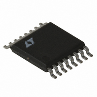
LT1766EFE#TRPBF Linear Technology, LT1766EFE#TRPBF Datasheet - Page 21

LT1766EFE#TRPBF
Manufacturer Part Number
LT1766EFE#TRPBF
Description
IC REG SW HV 1.5A 200KHZ 16TSSOP
Manufacturer
Linear Technology
Type
Step-Down (Buck)r
Datasheet
1.LT1766EGNPBF.pdf
(30 pages)
Specifications of LT1766EFE#TRPBF
Internal Switch(s)
Yes
Synchronous Rectifier
No
Number Of Outputs
1
Voltage - Output
1.2 ~ 54 V
Current - Output
1.5A
Frequency - Switching
200kHz
Voltage - Input
5.5 ~ 60 V
Operating Temperature
-40°C ~ 125°C
Mounting Type
Surface Mount
Package / Case
16-TSSOP Exposed Pad, 16-eTSSOP, 16-HTSSOP
Lead Free Status / RoHS Status
Lead free / RoHS Compliant
Power - Output
-
Available stocks
Company
Part Number
Manufacturer
Quantity
Price
APPLICATIONS INFORMATION
Thermal resistance for the LT1766 packages is infl uenced
by the presence of internal or backside planes.
SSOP (GN16) package: With a full plane under the GN16
package, thermal resistance will be about 85°C/W.
TSSOP (exposed pad) package: With a full plane under
the TSSOP package, thermal resistance will be about
45°C/W.
To calculate die temperature, use the proper thermal
resistance number for the desired package and add in
worst-case ambient temperature:
When estimating ambient, remember the nearby catch
diode and inductor will also be dissipating power:
Only a portion of the temperature rise in the external inductor
and diode is coupled to the junction of the LT1766. Based
on empirical measurements the thermal effect on LT1766
junction temperature due to power dissipation in the external
inductor and catch diode can be calculated as:
Using the example calculations for LT1766 dissipation, the
LT1766 die temperature will be estimated as:
With the GN16 package (θ
temperature of 60°C:
With the TSSOP package (θ
temperature of 60°C:
T
V
P
R
P
ΔT
T
T
T
P
P
J
DIODE
DIODE
J
J
J
F
INDUCTOR
INDUCTOR
L
= T
J
= T
= 60 + (85 • 0.53) + (10 • 0.65) = 112°C
= 60 + (45 • 0.53) + (10 • 0.65) = 90°C
= Forward voltage of diode (assume 0.63V at 1A)
= Inductor DC resistance (assume 0.1Ω)
(LT1766) ≈ (P
A
A
+ (θ
=
=
+ (θ
( )(
( . )(
0 63 40 5 1
V V
= (I
(1)
JA
JA
F
2
• P
LOAD
• P
(0.1) = 0.1W
IN
40
TOT
TOT
DIODE
–
)
2
V
– )( )
)
) + [10 • (P
V
IN
(R
OUT
+ P
L
JA
)
JA
)(
INDUCTOR
I
= 85°C/W), at an ambient
=
LOAD
= 45°C/W), at an ambient
0 55
.
DIODE
)
W
)(10°C/W)
+ P
INDUCTOR
)]
Die temperature can peak for certain combinations of V
V
switch AC losses, quiescent and catch diode losses, a
lower V
losses. In general, the maximum and minimum V
should be checked with maximum typical load current
for calculation of the LT1766 die temperature. If a more
accurate die temperature is required, a measurement of
the SYNC pin resistance (to GND) can be used. The SYNC
pin resistance can be measured by forcing a voltage no
greater than 0.5V at the pin and monitoring the pin cur-
rent over temperature in an oven. This should be done
with minimal device power (low V
(V
ambient (oven) temperature.
Note: Some of the internal power dissipation in the IC,
due to BOOST pin voltage, can be transferred outside
of the IC to reduce junction temperature, by increasing
the voltage drop in the path of the boost diode D2 (see
Figure 9). This reduction of junction temperature inside
the IC will allow higher ambient temperature operation for
a given set of conditions. BOOST pin circuitry dissipates
power given by:
Typically V
equals Vout. This is because diodes D1 and D2 can be
considered almost equal, where:
Hence the equation used for boost circuitry power dissi-
pation given in the previous Thermal Calculations section
is stated as:
Here it can be seen that boost power dissipation increases
as the square of V
below V
voltage drop in the path of D2. Care should be taken that
V
required for full saturation of the internal power switch.
OUT
C2
C
V
P
P
= 0V)) in order to calibrate SYNC pin resistance with
C2
does not fall below the minimum 3.3V boost voltage
DISS BOOST
DISS BOOST
and load current. While higher V
= V
IN
OUT
(
(
may generate greater losses due to switch DC
OUT
C2
to save power dissipation by increasing the
(the boost voltage across the capacitor C2)
– V
)
)
=
=
OUT
FD2
V
V
. It is possible, however, to reduce V
OUT
OUT
– (–V
LT1766/LT1766-5
• (
• (
I
I
FD1
SW
SW
V
V
IN
) = V
IN
/
/
36
36
)•
OUT
) •
IN
V
V
OUT
and no switching
C
IN
2
gives greater
IN
21
levels
1766fc
IN
C2
,


