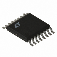
LT1766EFE#TRPBF Linear Technology, LT1766EFE#TRPBF Datasheet - Page 5

LT1766EFE#TRPBF
Manufacturer Part Number
LT1766EFE#TRPBF
Description
IC REG SW HV 1.5A 200KHZ 16TSSOP
Manufacturer
Linear Technology
Type
Step-Down (Buck)r
Datasheet
1.LT1766EGNPBF.pdf
(30 pages)
Specifications of LT1766EFE#TRPBF
Internal Switch(s)
Yes
Synchronous Rectifier
No
Number Of Outputs
1
Voltage - Output
1.2 ~ 54 V
Current - Output
1.5A
Frequency - Switching
200kHz
Voltage - Input
5.5 ~ 60 V
Operating Temperature
-40°C ~ 125°C
Mounting Type
Surface Mount
Package / Case
16-TSSOP Exposed Pad, 16-eTSSOP, 16-HTSSOP
Lead Free Status / RoHS Status
Lead free / RoHS Compliant
Power - Output
-
Available stocks
Company
Part Number
Manufacturer
Quantity
Price
ELECTRICAL CHARACTERISTICS
The
V
PARAMETER
f
f
Minimum Input Voltage
Minimum Boost Voltage
Boost Current (Note 5)
Input Supply Current (I
Bias Supply Current (I
Shutdown Supply Current
Lockout Threshold
Shutdown Thresholds
Minimum SYNC Amplitude
SYNC Frequency Range
SYNC Input Resistance
Note 1: Stresses beyond those listed under Absolute Maximum Ratings
may cause permanent damage to the device. Exposure to any Absolute
Maximum Rating condition for extended periods may affect device
reliability and lifetime.
Note 2: Gain is measured with a V
clamp level to 200mV below the upper clamp level.
Note 3: Minimum input voltage is not measured directly, but is guaranteed
by other tests. It is defi ned as the voltage where internal bias lines are still
regulated so that the reference voltage and oscillator remain constant.
Actual minimum input voltage to maintain a regulated output will depend
upon output voltage and load current. See Applications Information.
Note 4: This is the minimum voltage across the boost capacitor needed to
guarantee full saturation of the internal power switch.
Note 5: Boost current is the current fl owing into the BOOST pin with the
pin held 5V above input voltage. It fl ows only during switch on time.
Note 6: Input supply current is the quiescent current drawn by the input
pin when the BIAS pin is held at 5V with switching disabled. Bias supply
current is the current drawn by the BIAS pin when the BIAS pin is held
at 5V. Total input referred supply current is calculated by summing input
supply current (I
with V
SW
SW
IN
I
Line Regulation
Frequency Shifting Threshold
= 15V, V
TOTAL
l
IN
denotes specifi cations which apply over the full operating temperature range, otherwise specifi cations are at T
= 15V, V
= I
VIN
C
= 1.5V, SHDN = 1V, BOOST open circuit, SW open circuit, unless otherwise noted.
+ (I
VIN
OUT
) with a fraction of bias supply current (I
BIAS
= 5V, I
BIAS
VIN
)(V
)
)
OUT
VIN
/V
= 1.4mA, I
IN
C
)
swing equal to 200mV above the low
BIAS
= 2.9mA, I
CONDITIONS
5.5V ≤ V
Df = 10kHz
(Note 3)
(Note 4) I
Boost = V
Boost = V
(Note 6) V
(Note 6) V
SHDN = 0V, V
V
V
V
C
C
C
Open
Open, Shutting Down
Open, Starting Up
TOTAL
BIAS
IN
= 2.4mA.
SW
IN
IN
BIAS
BIAS
≤ 60V
):
+ 5V, I
+ 5V, I
≤ 0.75A
(LT1766H Grade)
IN
= 5V
= 5V
≤ 60V, SW = 0V, V
SW
SW
= 0.5A
= 0.75A
Note 7: Switch on-resistance is calculated by dividing V
by the forced current. See Typical Performance Characteristics for the
graph of switch voltage at other currents.
Note 8: The LT1766EGN, LT1766EGN-5, LT1766EFE and LT1766EFE-5
are guaranteed to meet performance specifi cations from 0°C to 125°C
junction temperature. Specifi cations over the –40°C to 125°C operating
junction temperature range are assured by design, characterization and
correlation with statistical process controls. The LT1766IGN, LT1766IGN-5,
LT1766IFE and LT1766IFE-5 are guaranteed over the full –40°C to 125°C
operating junction temperature range. The LT1766HGN and LT1766HFE are
guaranteed over the full –40°C to 140°C operating junction temperature
range.
Note 9: Transconductance and voltage gain refer to the internal amplifi er
exclusive of the voltage divider. To calculate gain and transconductance,
refer to the SENSE pin on fi xed voltage parts. Divide the values shown by
the ratio V
Note 10: This IC includes overtemperature protection that is intended
to protect the device during momentary overload conditions. Junction
temperature will exceed 140°C when overtemperature protection is active.
Continuous operation above the specifi ed maximum operating junction
temperature may impair device reliability.
Note 11: High junction temperatures degrade operating lifetimes.
Operating lifetime at junction temperatures between 125°C and 140°C is
derated to 1000 hours.
C
Open
OUT
/1.219.
l
l
l
l
l
l
l
l
l
l
LT1766/LT1766-5
0.15
0.25
MIN
228
2.3
0.05
2.42
0.37
0.45
TYP
0.8
4.6
1.8
1.4
2.9
1.5
12
45
25
20
J
IN
= 25°C.
MAX
0.15
2.68
100
120
500
700
to SW voltage
5.5
2.2
4.2
0.9
0.9
2.2
40
3
UNITS
1766fc
5
%/V
kHz
mA
mA
mA
mA
kΩ
μA
μA
V
V
V
V
V
V
V


