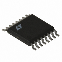
LT1766EFE#TRPBF Linear Technology, LT1766EFE#TRPBF Datasheet - Page 24

LT1766EFE#TRPBF
Manufacturer Part Number
LT1766EFE#TRPBF
Description
IC REG SW HV 1.5A 200KHZ 16TSSOP
Manufacturer
Linear Technology
Type
Step-Down (Buck)r
Datasheet
1.LT1766EGNPBF.pdf
(30 pages)
Specifications of LT1766EFE#TRPBF
Internal Switch(s)
Yes
Synchronous Rectifier
No
Number Of Outputs
1
Voltage - Output
1.2 ~ 54 V
Current - Output
1.5A
Frequency - Switching
200kHz
Voltage - Input
5.5 ~ 60 V
Operating Temperature
-40°C ~ 125°C
Mounting Type
Surface Mount
Package / Case
16-TSSOP Exposed Pad, 16-eTSSOP, 16-HTSSOP
Lead Free Status / RoHS Status
Lead free / RoHS Compliant
Power - Output
-
Available stocks
Company
Part Number
Manufacturer
Quantity
Price
LT1766/LT1766-5
APPLICATIONS INFORMATION
When using R
First, the combination of output capacitor ESR and R
may stop the loop rolling off altogether. Second, if the
loop gain is not rolled off suffi ciently at the switching
frequency, output ripple will peturb the V
cause unstable duty cycle switching similar to subharmonic
oscillations. If needed, an additional capacitor, C
added across the R
to further suppress V
With a tantalum output capacitor, the LT1766 already in-
cludes a resistor, R
(see Figures 10 and 11) to compensate the loop over the
entire V
V
still be used with a simple adjustment to the resistor R
for stable operation. (See Ceramic Capacitors section for
stabilizing LT1766). If additional phase margin is required,
a capacitor, C
pin but care must be taken for high output voltage applica-
tions. Sudden shorts to the output can create unacceptably
large negative transients on the FB pin.
For V
possible by readjusting the frequency compensation
components at the V
When checking loop stability, the circuit should be op-
erated over the applications’s full voltage, current and
temperature range. Proper loop compensation may be
obtained by emperical methods as described in detail in
Application Notes 19 and 76.
24
IN
-to-V
IN
-to-V
IN
OUT
range (to allow for stable pulse skipping for high
OUT
ratios ≥10). A ceramic output capacitor can
FB
C
, can be inserted between the output and FB
, the maximum value has two limitations.
ratios <10, higher loop bandwidths are
REMOVABLE
C
C
/C
and fi lter capacitor, C
C
INPUT
C
C
pin.
ripple voltage.
network from the V
10MQ060N
R3
54k
R4
25k
D3
Figure 12. Dual Source Supply with 25μA Reverse Leakage
C3
2.2μF
C
F
C
pin enough to
, at the V
pin to ground
V
SHDN
SYNC
GND
IN
0.022μF
F
, can be
BOOST
LT1766
2.2k
C
C
R
C
C
pin
C
C
BIAS
V
SW
C
FB
C
220pF
CONVERTER WITH BACKUP OUTPUT REGULATOR
In systems with a primary and backup supply, for example,
a battery-powered device with a wall adapter input, the
output of the LT1766 can be held up by the backup supply
with the LT1766 input disconnected. In this condition, the
SW pin will source current into the V
is held at ground, only the shut down current of 25μA will
be pulled via the SW pin from the second supply. With the
SHDN pin fl oating, the LT1766 will consume its quiescent
operating current of 1.5mA. The V
current to any other components connected to the input
line. If this load is greater than 10mA or the input could
be shorted to ground, a series Schottky diode must be
added, as shown in Figure 12. With these safeguards,
the output can be held at voltages up to the V
maximum rating.
BUCK CONVERTER WITH ADJUSTABLE SOFT-START
Large capacitive loads or high input voltages can cause
high input currents at start-up. Figure 13 shows a circuit
that limits the dv/dt of the output at start-up, controlling
the capacitor charge rate. The buck converter is a typical
confi guration with the addition of R3, R4, C
As the output starts to rise, Q1 turns on, regulating switch
current via the V
output. Output rise time is controlled by the current through
C
regulation, Q1 turns off and the circuit operates normally.
R3 is transient protection for the base of Q1.
0.33μF
F
SS
C2
defi ned by R4 and Q1’s V
D1
10MQ060N
47μH
L1
1N4148W
R1
15.4k
R2
4.99k
D2
C
pin to maintain a constant dv/dt at the
+
5V, 1A
C1
100μF
10V
BE
ALTERNATE
SUPPLY
. Once the output is in
IN
IN
1766 F12
pin will also source
pin. If the SHDN pin
SS
IN
absolute
and Q1.
1766fc


