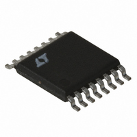
LT1766EFE#TRPBF Linear Technology, LT1766EFE#TRPBF Datasheet - Page 27

LT1766EFE#TRPBF
Manufacturer Part Number
LT1766EFE#TRPBF
Description
IC REG SW HV 1.5A 200KHZ 16TSSOP
Manufacturer
Linear Technology
Type
Step-Down (Buck)r
Datasheet
1.LT1766EGNPBF.pdf
(30 pages)
Specifications of LT1766EFE#TRPBF
Internal Switch(s)
Yes
Synchronous Rectifier
No
Number Of Outputs
1
Voltage - Output
1.2 ~ 54 V
Current - Output
1.5A
Frequency - Switching
200kHz
Voltage - Input
5.5 ~ 60 V
Operating Temperature
-40°C ~ 125°C
Mounting Type
Surface Mount
Package / Case
16-TSSOP Exposed Pad, 16-eTSSOP, 16-HTSSOP
Lead Free Status / RoHS Status
Lead free / RoHS Compliant
Power - Output
-
Available stocks
Company
Part Number
Manufacturer
Quantity
Price
APPLICATIONS INFORMATION
Note 44, pages 29 and 30. For our purposes here a fudge
factor (ff) is used. The value for ff is about 1.2 for higher
load currents and L ≥15μH. It increases to about 2.0 for
smaller inductors at lower load currents.
ff = 1.2 to 2.0
The output capacitor ripple current for the positive-to-
negative converter is similar to that for a typical buck
regulator—it is a triangular waveform with peak-to-peak
value equal to the peak-to-peak triangular waveform of the
inductor. The low output ripple design in Figure 15 places
the input capacitor between V
output. This placement of the input capacitor signifi cantly
reduces the size required for the output capacitor (versus
placing the input capacitor between V
The peak-to-peak ripple current in both the inductor and
output capacitor (assuming continuous mode) is:
The output ripple voltage for this confi guration is as low
as the typical buck regulator based predominantly on the
inductor’s triangular peak-to-peak ripple current and the
ESR of the chosen capacitor (see Output Ripple Voltage
in Applications Information).
Diode Current
Average diode current is equal to load current. Peak diode
current will be considerably higher.
Peak diode current:
Input Capacitor I
I
DC Duty Cycle
I
I
Discontinuous Mode
Continuous Mode
P-P
COUT
OUT
=
=
(
V
(
DC V
RMS
IN
f L
+
V
•
•
IN
V
)
IN
OUT
=
I
P-P
)
RMS
=
12
+
=
V
2
OUT
( )( )(
=
= ( )(
L f V
V
OUT
(
V
ff I
+
IN
IN
2
V
(
and the regulated negative
I
+
)(
IN
OUT
OUT
IN
V
V
( )( )
+
OUT
L f
F
+
)(
)
V
V
F
V
IN
OUT
)
OUT
V
V
OUT
and ground).
IN
)
)
Keep in mind that during start-up and output overloads,
average diode current may be much higher than with nor-
mal loads. Care should be used if diodes rated less than
1A are used, especially if continuous overload conditions
must be tolerated.
BOOST Pin Voltage
To ensure that the BOOST pin voltage does not exceed its
absolute maximum rating of 68V with respect to device
GND pin voltage, care should be taken in the generation of
boost voltage. For the conventional method of generating
boost voltage, shown in Figure 1, the voltage at the BOOST
pin during switch on time is approximately given by:
where:
For the positive-to-negative converter shown in Figure 15,
the conventional Buck output node is grounded (D2+) = 0V
and the catch diode (D1+) is connected to the negative
output = V
also be observed with the GND pin now at –12V. It can be
seen that for V
The maximum V
pin at –12V) is 48V.
The maximum V
BOOST pin voltage absolute maximum rating is given by:
To increase usable V
can be achieved by placing a zener diode V
C2+) in series with D2.
Note: A maximum limit on V
ensure a minimum V
capacitor; referred to as V
Characteristics.
V
V
V
V
V
BOOST
C2
C2
IN(MAX)
IN(MAX)
= (D2+) – V
= (D2+) – (D1+) = |V
= voltage across the boost capacitor
OUT
(GND pin) = (V
= Boost (Max) + (V
= 68 + (–12) – 12 = 44V
= –12V. Absolute maximum ratings should
D1
IN
IN
= V
D2
voltage allowed without exceeding the
voltage allowed for the device (GND
IN
D2
– (D1+) + V
voltage, V
:
C2
LT1766/LT1766-5
IN
is maintained on the boost
OUT
– V
BOOST(MIN)
GNDPIN
Z1
| = 12V
GNDPIN
C2
D1
must be observed to
must be reduced. This
) – V
) + V
in the Electrical
C2
C2
Z1
(anode at
27
1766fc


