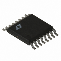
LT1766EFE#TRPBF Linear Technology, LT1766EFE#TRPBF Datasheet - Page 8

LT1766EFE#TRPBF
Manufacturer Part Number
LT1766EFE#TRPBF
Description
IC REG SW HV 1.5A 200KHZ 16TSSOP
Manufacturer
Linear Technology
Type
Step-Down (Buck)r
Datasheet
1.LT1766EGNPBF.pdf
(30 pages)
Specifications of LT1766EFE#TRPBF
Internal Switch(s)
Yes
Synchronous Rectifier
No
Number Of Outputs
1
Voltage - Output
1.2 ~ 54 V
Current - Output
1.5A
Frequency - Switching
200kHz
Voltage - Input
5.5 ~ 60 V
Operating Temperature
-40°C ~ 125°C
Mounting Type
Surface Mount
Package / Case
16-TSSOP Exposed Pad, 16-eTSSOP, 16-HTSSOP
Lead Free Status / RoHS Status
Lead free / RoHS Compliant
Power - Output
-
Available stocks
Company
Part Number
Manufacturer
Quantity
Price
PIN FUNCTIONS
BLOCK DIAGRAM
LT1766/LT1766-5
switch. V
voltage on the BIAS pin is not present. High dI/dt edges
occur on this pin during switch turn on and off. Keep
the path short from the V
capacitor, through the catch diode back to SW. All trace
inductance on this path will create a voltage spike at switch
off, adding to the V
BOOST (Pin 6): The BOOST pin is used to provide a drive
voltage, higher than the input voltage, to the internal bipolar
NPN power switch. Without this added voltage, the typical
switch voltage loss would be about 1.5V. The additional
BOOST voltage allows the switch to saturate and voltage
loss approximates that of a 0.2Ω FET structure, but with
much smaller die area.
BIAS (Pin 10): The BIAS pin is used to improve effi ciency
when operating at higher input voltages and light load cur-
rent. Connecting this pin to the regulated output voltage
forces most of the internal circuitry to draw its operating
current from the output voltage rather than the input supply.
This architecture increases effi ciency especially when the
input voltage is much higher than the output. Minimum
output voltage setting for this mode of operation is 3V.
V
and the input of the peak switch current comparator. It is
normally used for frequency compensation, but can also
serve as a current clamp or control loop override. V
at about 0.9V for light loads and 2.1V at maximum load.
It can be driven to ground to shut off the regulator, but if
driven high, current must be limited to 4mA.
The LT1766 is a constant frequency, current mode buck
converter. This means that there is an internal clock and
two feedback loops that control the duty cycle of the power
switch. In addition to the normal error amplifi er, there is a
current sense amplifi er that monitors switch current on a
cycle-by-cycle basis. A switch cycle starts with an oscillator
pulse which sets the R
switch current reaches a level set by the inverting input of
8
V
C
IN
(Pin 11) The V
(Pin 4): This is the collector of the on-chip power NPN
IN
powers the internal control circuitry when a
C
CE
pin is the output of the error amplifi er
S
voltage across the internal NPN.
fl ip-fl op to turn the switch on. When
IN
pin through the input bypass
C
sits
FB/SENSE (Pin 12): The feedback pin is used to set the
output voltage using an external voltage divider that gener-
ates 1.22V at the pin for the desired output voltage. The
5V fi xed output voltage parts have the divider included on
the chip and the FB pin is used as a SENSE pin, connected
directly to the 5V output. Three additional functions are
performed by the FB pin. When the pin voltage drops below
0.6V, switch current limit is reduced and the external SYNC
function is disabled. Below 0.8V, switching frequency is
also reduced. See Feedback Pin Functions in Applications
Information for details.
SYNC (Pin 14): The SYNC pin is used to synchronize the
internal oscillator to an external signal. It is directly logic
compatible and can be driven with any signal between 10%
and 90% duty cycle. The synchronizing range is equal to
initial operating frequency up to 700kHz. See Synchroniz-
ing in Applications Information for details.
SHDN (Pin 15): The SHDN pin is used to turn off the
regulator and to reduce input drain current to a few mi-
croamperes. This pin has two thresholds: one at 2.38V to
disable switching and a second at 0.4V to force complete
micropower shutdown. The 2.38V threshold functions
as an accurate undervoltage lockout (UVLO); sometimes
used to prevent the regulator from delivering power until
the input voltage has reached a predetermined level.
If the SHDN pin functions are not required, the pin can
either be left open (to allow an internal bias current to lift
the pin to a default high state) or be forced high to a level
not to exceed 6V.
the comparator, the fl ip-fl op is reset and the switch turns
off. Output voltage control is obtained by using the output
of the error amplifi er to set the switch current trip point.
This technique means that the error amplifi er commands
current to be delivered to the output rather than voltage.
A voltage fed system will have low phase shift up to the
resonant frequency of the inductor and output capacitor,
then an abrupt 180° shift will occur. The current fed system
1766fc


