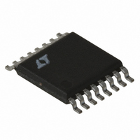
LT1766EFE#TRPBF Linear Technology, LT1766EFE#TRPBF Datasheet - Page 20

LT1766EFE#TRPBF
Manufacturer Part Number
LT1766EFE#TRPBF
Description
IC REG SW HV 1.5A 200KHZ 16TSSOP
Manufacturer
Linear Technology
Type
Step-Down (Buck)r
Datasheet
1.LT1766EGNPBF.pdf
(30 pages)
Specifications of LT1766EFE#TRPBF
Internal Switch(s)
Yes
Synchronous Rectifier
No
Number Of Outputs
1
Voltage - Output
1.2 ~ 54 V
Current - Output
1.5A
Frequency - Switching
200kHz
Voltage - Input
5.5 ~ 60 V
Operating Temperature
-40°C ~ 125°C
Mounting Type
Surface Mount
Package / Case
16-TSSOP Exposed Pad, 16-eTSSOP, 16-HTSSOP
Lead Free Status / RoHS Status
Lead free / RoHS Compliant
Power - Output
-
Available stocks
Company
Part Number
Manufacturer
Quantity
Price
LT1766/LT1766-5
APPLICATIONS INFORMATION
a >100MHz oscilloscope must be used, and waveforms
should be observed on the leads of the package. This
switch off spike will also cause the SW node to go below
ground. The LT1766 has special circuitry inside which
mitigates this problem, but negative voltages over 0.8V
lasting longer than 10ns should be avoided. Note that
100MHz oscilloscopes are barely fast enough to see the
details of the falling edge overshoot in Figure 7.
A second, much lower frequency ringing is seen during
switch off-time if load current is low enough to allow the
inductor current to fall to zero during part of the switch
off-time (see Figure 8). Switch and diode capacitance
resonate with the inductor to form damped ringing at 1MHz
to 10 MHz. This ringing is not harmful to the regulator
and it has not been shown to contribute signifi cantly to
EMI. Any attempt to damp it with a resistive snubber will
degrade effi ciency.
THERMAL CALCULATIONS
Power dissipation in the LT1766 chip comes from four
sources: switch DC loss, switch AC loss, boost circuit cur-
rent, and input quiescent current. The following formulas
show how to calculate each of these losses. These formulas
assume continuous mode operation, so they should not
be used for calculating effi ciency at light load currents.
Switch loss:
20
P
SW
=
2V/DIV
R
SW OUT
Figure 7. Switch Node Resonance
( ) ( )
I
V
SW RISE
IN
2
V
OUT
50ns/DIV
SW FALL
+
t
EFF
( / )
1 2
1766 F07
( )( )( )
I
OUT
V
IN
f
Boost current loss:
Quiescent current loss:
Example: with V
Total power dissipation in the IC is given by:
P
P
P
SW
Q
BOOST
R
t
t
t
t
f = Switch frequency
P
P
P
EFF
r
f
Ir
=
Q
BOOST
SW
TOT
= (V
= (V
= t
=
=
40 0 0015
=
0.2A/DIV
= Effective switch current/voltage overlap time
10V/DIV
= (t
0 04 0 388 0 43
= Switch resistance (≈ 0.3) hot
( )( ) ( )
If
= P
= 0.43W + 0.02W + 0.08W = 0.53W
V
=
( .
0 3 1 5
IN
IN
.
IN
= (I
.
r
/1.7)ns
/1.2)ns
( ) (
=
Figure 8. Discontinuous Mode Ringing
(
5
SW
+ t
0 0015
40
+
V
V
L = 47μH
OUT
V
IN
OUT
.
2
OUT
f
40
+ P
= 40V
2
+ t
1 36
.
IN
= 5V
/0.05)ns
)
/
+
2
BOOST
Ir
= 40V, V
(
V
)
5 0 003
I
+ t
+
OUT
)
( .
IN
+
=
(
=
If
V
97 10
)
OUT
.
0 02
+ P
/
1μs/DIV
36
•
.
OUT
)
W
Q
(
)
0 003
W
=
−
.
= 5V and I
9
0 08
)
.
( ) ( )( )
1 2 1 40 200 10
/
)
W
1766 F08
OUT
SWITCH NODE
VOLTAGE
INDUCTOR
CURRENT
AT I
= 1A:
(
OUT
= 0.1A
•
1766fc
3
)


