EVL250W-ATX80PL STMicroelectronics, EVL250W-ATX80PL Datasheet - Page 12
EVL250W-ATX80PL
Manufacturer Part Number
EVL250W-ATX80PL
Description
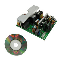
BOARD DEMO SMPS L6591/L6563S
Manufacturer
STMicroelectronics
Series
VIPer™ plusr
Datasheet
1.EVL250W-ATX80PL.pdf
(45 pages)
Specifications of EVL250W-ATX80PL
Main Purpose
Power Supply, ATX
Outputs And Type
3, Isolated
Power - Output
250W
Voltage - Output
12V, 5V, 3.3V
Current - Output
13.5A, 12A, 8A
Voltage - Input
88 ~ 264VAC
Regulator Topology
Flyback
Frequency - Switching
80kHz
Board Type
Fully Populated
Utilized Ic / Part
L6563S, L6591, L6727, VIPer27H
Input Voltage
88 VAC to 264 VAC
Output Voltage
3.3 V, 5 V, 12 V
Maximum Operating Temperature
+ 60 C
Operating Supply Voltage
80 VAC to 264 VAC
Output Power
250 W
Product
Power Management Development Tools
Lead Free Status / RoHS Status
Lead free / RoHS Compliant
For Use With/related Products
L6563S PFC controller
Other names
497-10596


Asymmetrical half bridge operation
2
2.1
12/45
Asymmetrical half bridge operation
AHB typical waveforms
In
applied are shown.
cycle.
The AHB stage has been designed to operate at about 80 kHz with a nominal input voltage
of 400 V (PFC output bus). The transformer design is the result of a trade-off between the
half bridge MOSFETs zero voltage switching (ZVS) operation requirements, the primary rms
current, and duty cycle losses. In fact, ZVS can be achieved by reducing the magnetizing
inductance or increasing the leakage inductance. With the output power of this board, the
first solution implies having very high rms primary current which leads to high losses. The
second solution introduces the so called “duty cycle losses”. When the leakage inductance
is de-magnetizing, the voltages on the secondary side windings are zero and therefore the
output mean value is reduced with respect to the same half bridge duty cycle and negligible
leakage inductance. Duty cycle losses limit the hold-up capability of the power supply
because they increase the minimum input voltage that guarantees output regulation.
In this design the system works with ZVS for both MOSFETs at full load. Because of the
intrinsic asymmetry of the topology the behavior of the two switches is different. When the
load is reduced the low side MOSFET always operates in ZVS while the high side one starts
loosing ZVS. The high side MOSFET never turns on with full bus voltage applied between its
drain and source. As shown in
about 100 V, definitely lower compared with the 400 V of a hard switching solution.
This design can therefore meet both efficiency and dynamic requirements.
Figure 6.
Ch1: LVG pin voltage (yellow)
Ch3: HVG pin voltage (purple)
Ch4: Primary winding current (green)
Figure 6
the primary side key waveforms during steady-state operation with full load
AHB primary side key waveforms @ full load
Figure 7
shows the detail of the two transitions during one switching
Doc ID 17402 Rev 1
Figure
8, even at 20 % of rated load the Vds at turn-on is
AN3203
Related parts for EVL250W-ATX80PL
Image
Part Number
Description
Manufacturer
Datasheet
Request
R

Part Number:
Description:
STMicroelectronics [RIPPLE-CARRY BINARY COUNTER/DIVIDERS]
Manufacturer:
STMicroelectronics
Datasheet:
Part Number:
Description:
STMicroelectronics [LIQUID-CRYSTAL DISPLAY DRIVERS]
Manufacturer:
STMicroelectronics
Datasheet:

Part Number:
Description:
BOARD EVAL FOR MEMS SENSORS
Manufacturer:
STMicroelectronics
Datasheet:
Part Number:
Description:
NPN TRANSISTOR POWER MODULE
Manufacturer:
STMicroelectronics
Datasheet:
Part Number:
Description:
TURBOSWITCH ULTRA-FAST HIGH VOLTAGE DIODE
Manufacturer:
STMicroelectronics
Datasheet:
Part Number:
Description:
Manufacturer:
STMicroelectronics
Datasheet:
Part Number:
Description:
DIODE / SCR MODULE
Manufacturer:
STMicroelectronics
Datasheet:
Part Number:
Description:
DIODE / SCR MODULE
Manufacturer:
STMicroelectronics
Datasheet:
Part Number:
Description:
Search -----> STE16N100
Manufacturer:
STMicroelectronics
Datasheet:
Part Number:
Description:
Search ---> STE53NA50
Manufacturer:
STMicroelectronics
Datasheet:
Part Number:
Description:
NPN Transistor Power Module
Manufacturer:
STMicroelectronics
Datasheet:
Part Number:
Description:
DIODE / SCR MODULE
Manufacturer:
STMicroelectronics
Datasheet: