Z8F16800144ZCOG Zilog, Z8F16800144ZCOG Datasheet - Page 238
Z8F16800144ZCOG
Manufacturer Part Number
Z8F16800144ZCOG
Description
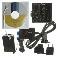
KIT DEV FOR Z8F642 MCU 44 PIN
Manufacturer
Zilog
Series
Z8 Encore!®r
Type
MCUr
Specifications of Z8F16800144ZCOG
Contents
Hardware, Software and Documentation
For Use With/related Products
Z8F642
For Use With
269-4661 - KIT ACC ETHERNET SMART CABLE
Lead Free Status / RoHS Status
Lead free / RoHS Compliant
Other names
269-4678


PS025011-1010
S
Slave Address
1st Byte
Figure 44. Data Transfer Format—Master Write Transaction with a 10-Bit Address
The first 7 bits transmitted in the first byte are
significant bits of the 10-bit address. The lowest bit of the first byte transferred is the
Read/Write control bit (which is cleared to 0). The transmit operation is performed in the
same manner as 7-bit addressing.
Follow the steps below for a master transmit operation to a 10-bit addressed slave:
1. The software initializes the
2. The software asserts the
3. The I
4. The software responds to the TDRE interrupt by writing the first Slave Address byte
5. The software asserts the
6. The I
7. The I
8. After one bit of the address is shifted out by the SDA signal, the transmit interrupt
9. The software responds by writing the second byte of address into the contents
10. The I
11. The I
MASTER/SLAVE mode with 7- or 10-bit addressing (the I
mixing of slave address types). The
when addressed as a slave (but not for the remote slave). The software asserts the IEN
bit in the I
interrupts.
(
I
asserts.
of the I
the Write bit out via the SDA signal.
high period of SCL. The I
If the slave does not acknowledge the first address byte, the I
the NCKI bit in the I
the I
setting the
address byte from the data register, sends a
11110xx0
2
C Data Register.
2
2
2
2
2
2
C State Register. The software responds to the Not Acknowledge interrupt by
C interrupt asserts because the I
C controller sends a
C controller loads the I
C controller shifts the remainder of the first byte of the address and
C slave sends an Acknowledge by pulling the SDA signal Low during the next
W = 0
2
C Data Register.
2
STOP
C Control Register.
). The least-significant bit must be 0 for the write operation.
A
bit and clearing the
2
Slave Address
C Status Register, sets the
P R E L I M I N A R Y
2nd Byte
TXI
START
2
START
C controller sets the ACK bit in the I
MODE
bit of the I
2
C Shift Register with the contents of the
bit of the I
field in the I
condition to the I
MODE
TXI
2
A
C Data Register is empty.
2
C Control Register to enable transmit
bit. The I
field selects the address width for this mode
11110XX
2
STOP
C Control Register.
Data
2
C Mode Register for
ACKV
condition on the bus, and clears
2
2
Z8 Encore! XP
C controller flushes the second
. The 2
C Slave.
A
bit, and clears the
2
XX
C bus protocol allows the
Product Specification
Data
I2C Master/Slave Controller
2
C controller sets
bits are the two most
2
C Status Register.
®
F1680 Series
A/A
ACK
bit in
F/S
224
Related parts for Z8F16800144ZCOG
Image
Part Number
Description
Manufacturer
Datasheet
Request
R

Part Number:
Description:
Communication Controllers, ZILOG INTELLIGENT PERIPHERAL CONTROLLER (ZIP)
Manufacturer:
Zilog, Inc.
Datasheet:

Part Number:
Description:
KIT DEV FOR Z8 ENCORE 16K TO 64K
Manufacturer:
Zilog
Datasheet:

Part Number:
Description:
KIT DEV Z8 ENCORE XP 28-PIN
Manufacturer:
Zilog
Datasheet:

Part Number:
Description:
DEV KIT FOR Z8 ENCORE 8K/4K
Manufacturer:
Zilog
Datasheet:

Part Number:
Description:
KIT DEV Z8 ENCORE XP 28-PIN
Manufacturer:
Zilog
Datasheet:

Part Number:
Description:
DEV KIT FOR Z8 ENCORE 4K TO 8K
Manufacturer:
Zilog
Datasheet:
Part Number:
Description:
CMOS Z8 microcontroller. ROM 16 Kbytes, RAM 256 bytes, speed 16 MHz, 32 lines I/O, 3.0V to 5.5V
Manufacturer:
Zilog, Inc.
Datasheet:
Part Number:
Description:
Low-cost microcontroller. 512 bytes ROM, 61 bytes RAM, 8 MHz
Manufacturer:
Zilog, Inc.
Datasheet:
Part Number:
Description:
Z8 4K OTP Microcontroller
Manufacturer:
Zilog, Inc.
Datasheet:
Part Number:
Description:
CMOS SUPER8 ROMLESS MCU
Manufacturer:
Zilog, Inc.
Datasheet:
Part Number:
Description:
SL1866 CMOSZ8 OTP Microcontroller
Manufacturer:
Zilog, Inc.
Datasheet:
Part Number:
Description:
SL1866 CMOSZ8 OTP Microcontroller
Manufacturer:
Zilog, Inc.
Datasheet:
Part Number:
Description:
OTP (KB) = 1, RAM = 125, Speed = 12, I/O = 14, 8-bit Timers = 2, Comm Interfaces Other Features = Por, LV Protect, Voltage = 4.5-5.5V
Manufacturer:
Zilog, Inc.
Datasheet:
Part Number:
Description:
Manufacturer:
Zilog, Inc.
Datasheet: