FIN1019M Fairchild Semiconductor, FIN1019M Datasheet
FIN1019M
Specifications of FIN1019M
FIN1019M_NL
Available stocks


Related parts for FIN1019M


FIN1019M Summary of contents
Page 1
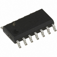
... FIN1019M M14A 14-Lead Small Outline Integrated Circuit (SOIC), JEDEC MS-012, 0.150" Narrow FIN1019MTC MTC14 14-Lead Thin Shrink Small Outline Package (TSSOP), JEDEC MO-153, 4.4mm Wide Devices also available in Tape and Reel. Specify by appending the suffix letter “X” to the ordering code. ...
Page 2
Absolute Maximum Ratings Supply Voltage ( LVTTL DC Input Voltage (D , DE, RE) IN LVDS DC Input Voltage ( LVTTL DC Output Voltage (R ) OUT LVDS DC Output Voltage (D , ...
Page 3
DC Electrical Characteristics Device Characteristics I Power Supply Current CC C Input Capacitance IN C Output Capacitance OUT Note 2: All typical values are and with Electrical Characteristics Over supply voltage and ...
Page 4
FIGURE 1. Differential Driver DC Test Circuit FIGURE 3. AC Waveforms for Differential Driver FIGURE 5. Enable and Disable AC Waveforms www.fairchildsemi.com Note A: Input pulses have frequency 10 MHz Note B: C includes all probe ...
Page 5
Note A: Input pulses have frequency 10 MHz Note B: C includes all probe and fixture capacitance L FIGURE 6. Differential Receiver Voltage Definitions and Propagation Delay and Transition Time Test Circuit TABLE 1. Receiver ...
Page 6
FIGURE 7. LVDS Input to LVTTL Output AC Waveforms Voltage Waveforms Enable and Disable Times FIGURE 8. LVTTL Outputs Test Circuit and AC Waveforms www.fairchildsemi.com Test Circuit for LVTTL Outputs 6 ...
Page 7
Typical Performance Curves Drivers FIGURE 9. Output High Voltage vs. Power Supply Voltage FIGURE 11. Output Short Circuit Current vs. Power Supply Voltage FIGURE 13. Differential Output Voltage vs. Load Resistor FIGURE 10. Output Low Voltage vs. ...
Page 8
Typical Performance Curves FIGURE 15. Power Supply Current vs. Frequency FIGURE 17. Power Supply Current vs. Ambient Temperature FIGURE 19. Differential Propagation Delay vs. Ambient Temperature www.fairchildsemi.com (Continued) FIGURE 16. Power Supply Current vs. Power Supply Voltage ...
Page 9
Typical Performance Curves FIGURE 21. Differential Pulse Skew (t PLH Ambient Temperature (Continued vs. PHL FIGURE 22. Transition Time vs. Power Supply Voltage FIGURE 23. Transition Times vs. Ambient Temperature 9 www.fairchildsemi.com ...
Page 10
Typical Performance Curves Receiver FIGURE 24. Output High Voltage vs. Power Supply Voltage FIGURE 26. Output Short Circuit Current vs. Power Supply Voltage FIGURE 28. Power Supply Current vs. Power Supply Voltage www.fairchildsemi.com FIGURE 25. Output Low ...
Page 11
Typical Performance Curves FIGURE 30. Differential Propagation Delay vs. Power Supply Voltage FIGURE 32. Differential Skew ( PHL Power Supply Voltage FIGURE 34. Differential Propagation Delay vs. Differential Input Voltage (Continued) FIGURE 31. Differential Propagation ...
Page 12
Typical Performance Curves FIGURE 36. Transition Time vs. Power Supply Voltage FIGURE 38. Differential Propagation Delay vs. Load www.fairchildsemi.com (Continued) FIGURE 37. Transition Time vs. Ambient Temperature FIGURE 39. Transition Time vs. Load 12 ...
Page 13
Physical Dimensions inches (millimeters) unless otherwise noted 14-Lead Small Outline Integrated Circuit (SOIC), JEDEC MS-012, 0.150" Narrow Package Number M14A 13 www.fairchildsemi.com ...
Page 14
Physical Dimensions inches (millimeters) unless otherwise noted (Continued) 14-Lead Thin Shrink Small Outline Package (TSSOP), JEDEC MO-153, 4.4mm Wide Fairchild does not assume any responsibility for use of any circuitry described, no circuit patent licenses are implied and Fairchild reserves ...