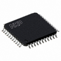
P89LV51RD2BBC,557 NXP Semiconductors, P89LV51RD2BBC,557 Datasheet - Page 16

P89LV51RD2BBC,557
Manufacturer Part Number
P89LV51RD2BBC,557
Description
IC 80C51 MCU FLASH 64K 44-TQFP
Manufacturer
NXP Semiconductors
Series
89LVr
Datasheet
1.P89LV51RD2BBC557.pdf
(76 pages)
Specifications of P89LV51RD2BBC,557
Program Memory Type
FLASH
Program Memory Size
64KB (64K x 8)
Package / Case
44-TQFP, 44-VQFP
Core Processor
8051
Core Size
8-Bit
Speed
33MHz
Connectivity
SPI, UART/USART
Peripherals
Brown-out Detect/Reset, POR, PWM, WDT
Number Of I /o
32
Ram Size
1K x 8
Voltage - Supply (vcc/vdd)
2.7 V ~ 3.6 V
Oscillator Type
Internal
Operating Temperature
0°C ~ 70°C
Processor Series
P89LV5x
Core
80C51
Data Bus Width
8 bit
Data Ram Size
1 KB
Interface Type
SPI/UART
Maximum Clock Frequency
40 MHz
Number Of Programmable I/os
32
Number Of Timers
3
Operating Supply Voltage
2.7 V to 3.6 V
Maximum Operating Temperature
+ 70 C
Mounting Style
SMD/SMT
3rd Party Development Tools
PK51, CA51, A51, ULINK2
Minimum Operating Temperature
0 C
Cpu Family
89LV
Device Core
80C51
Device Core Size
8b
Frequency (max)
40MHz
Total Internal Ram Size
1KB
# I/os (max)
32
Number Of Timers - General Purpose
3
Operating Supply Voltage (typ)
3.3V
Operating Supply Voltage (max)
3.6V
Operating Supply Voltage (min)
2.7V
Instruction Set Architecture
CISC
Operating Temp Range
0C to 70C
Operating Temperature Classification
Commercial
Mounting
Surface Mount
Pin Count
44
Package Type
TQFP
Lead Free Status / RoHS Status
Lead free / RoHS Compliant
For Use With
622-1017 - BOARD 44-ZIF PLCC SOCKET622-1008 - BOARD FOR LPC9103 10-HVSON622-1001 - USB IN-CIRCUIT PROG 80C51ISP
Eeprom Size
-
Data Converters
-
Lead Free Status / Rohs Status
Lead free / RoHS Compliant
Other names
568-1289
935274177557
P89LV51RD2BBC
935274177557
P89LV51RD2BBC
Available stocks
Company
Part Number
Manufacturer
Quantity
Price
Company:
Part Number:
P89LV51RD2BBC,557
Manufacturer:
NXP Semiconductors
Quantity:
10 000
NXP Semiconductors
Table 6.
P89LV51RB2_RC2_RD2_5
Product data sheet
Reset source
External reset
Power-on reset
Watchdog reset
Brownout detect reset
Software reset
Effects of reset sources on bank selection
6.2.5 Watchdog reset
6.2.6 Data RAM memory
6.2.7 Expanded data RAM addressing
V
detection circuit will respond.
Brownout interrupt can be enabled by setting the EBO bit (IEN1.3). If EBO bit is set and a
brownout condition occurs, a brownout interrupt will be generated to execute the program
at location 004BH. It is required that the EBO bit is cleared by software after the brownout
interrupt is serviced. Clearing EBO bit when the brownout condition is active will properly
reset the device. If brownout interrupt is not enabled, a brownout condition will reset the
program to resume execution at location 0000H. A brownout detect reset will clear the
BSEL bit (FCF.0) but will not change the SWR bit (FCF.1) and therefore will not change the
banking of the lower 8 kB of user code memory space.
Like a brownout detect reset, the watchdog timer reset will clear the BSEL bit (FCF.0) but
will not change the SWR bit (FCF.1) and therefore will not change the banking of the lower
8 kB of user code memory space.
The state of the SWR and BSEL bits after different types of resets is shown in
This results in the code memory bank selections as shown.
The data RAM has 1024 B of internal memory. The device can also address up to 64 kB
for external data memory.
The P89LV51RB2/RC2/RD2 has 1 kB of RAM. See
memory structure” on page
The device has four sections of internal data memory:
SWR bit result
(FCF.1)
0
x
1
1. The lower 128 B of RAM (00H to 7FH) are directly and indirectly addressable.
2. The higher 128 B of RAM (80H to FFH) are indirectly addressable.
3. The special function registers (80H to FFH) are directly addressable only.
4. The expanded RAM of 768 B (00H to 2FFH) is indirectly addressable by the move
DD
external instruction (MOVX) and clearing the EXTRAM bit (see ‘Auxiliary function
Register’ (AUXR) in
must stay below V
BSEL bit result
(FCF.0)
0
0
0
Rev. 05 — 15 December 2009
bo
Table 4 “Special function registers” on page
at least four oscillator clock periods before the brownout
19.
Addresses from 0000H to
1FFFH
Boot code (in block 1)
Retains state of SWR bit. If
SWR, BSEL = 00 then uses
boot code. If SWR,
BSEL = 10 then uses user
code.
User code (in block 0)
P89LV51RB2/RC2/RD2
8-bit microcontrollers with 80C51 core
Figure 5 “Internal and external data
Addresses above
1FFFH
User code (in block 0)
11).
© NXP B.V. 2009. All rights reserved.
Table
16 of 76
6.


